NMOS device, PMOS device, and SiGe HBT device formed on SOI substrate and method of fabricating the same

a technology of pmos and soi substrate, which is applied in the direction of semiconductor devices, electrical devices, transistors, etc., can solve the problems of increasing the heat in the chip, becoming an obstacle to practically using the device, and increasing the use of the soi substrate in the cmos, so as to improve the drain breakdown voltage, reduce the sub-threshold leakage current, and reduce the leakage current. , the effect of lowering the dibl

Active Publication Date: 2005-06-30
ELECTRONICS & TELECOMM RES INST
View PDF5 Cites 52 Cited by
  • Summary
  • Abstract
  • Description
  • Claims
  • Application Information

AI Technical Summary

Benefits of technology

[0008] The present invention is directed to a SiGe BiCMOS device which has advantages of suppressing a drain induces barrier lowering (DIBL) leakage current, improving a drain breakdown voltage, reducing a sub-threshold leakage current, and reducing a body effect, and a method of fabricating the same.
[0009] The present invention is also directed to an NMOS device, a PMOS device and a SiGe HBT device which prevents a leakage current and improves a heat dissipation characteristic without reducing an effective operation range of a CMOS and a method of fabricating the same.

Problems solved by technology

Meanwhile, a use of the SOI substrate in the CMOS is increasing due to low power consumption.
However, as a gate length is scaled down to less than 100 nm in such structure, an abnormal leakage current is increased due to parasitic bipolar operation between a source and a drain, and a resistance of the source and drain layer and a resistance between the source and drain layer and a contact point with an external metal line are sharply increased, and thus heat in the chip is increased.
This becomes an obstacle to practically using the device.

Method used


Image

  • NMOS device, PMOS device, and SiGe HBT device formed on SOI substrate and method of fabricating the same
  • NMOS device, PMOS device, and SiGe HBT device formed on SOI substrate and method of fabricating the same
  • NMOS device, PMOS device, and SiGe HBT device formed on SOI substrate and method of fabricating the same

Examples


Embodiment Construction

[0021] Reference will now be made in detail to the embodiments of the present invention, examples of which are illustrated in the accompanying drawings, wherein like reference numerals refer to the like elements throughout. The embodiments are described below in order to explain the present invention by referring to the figures.

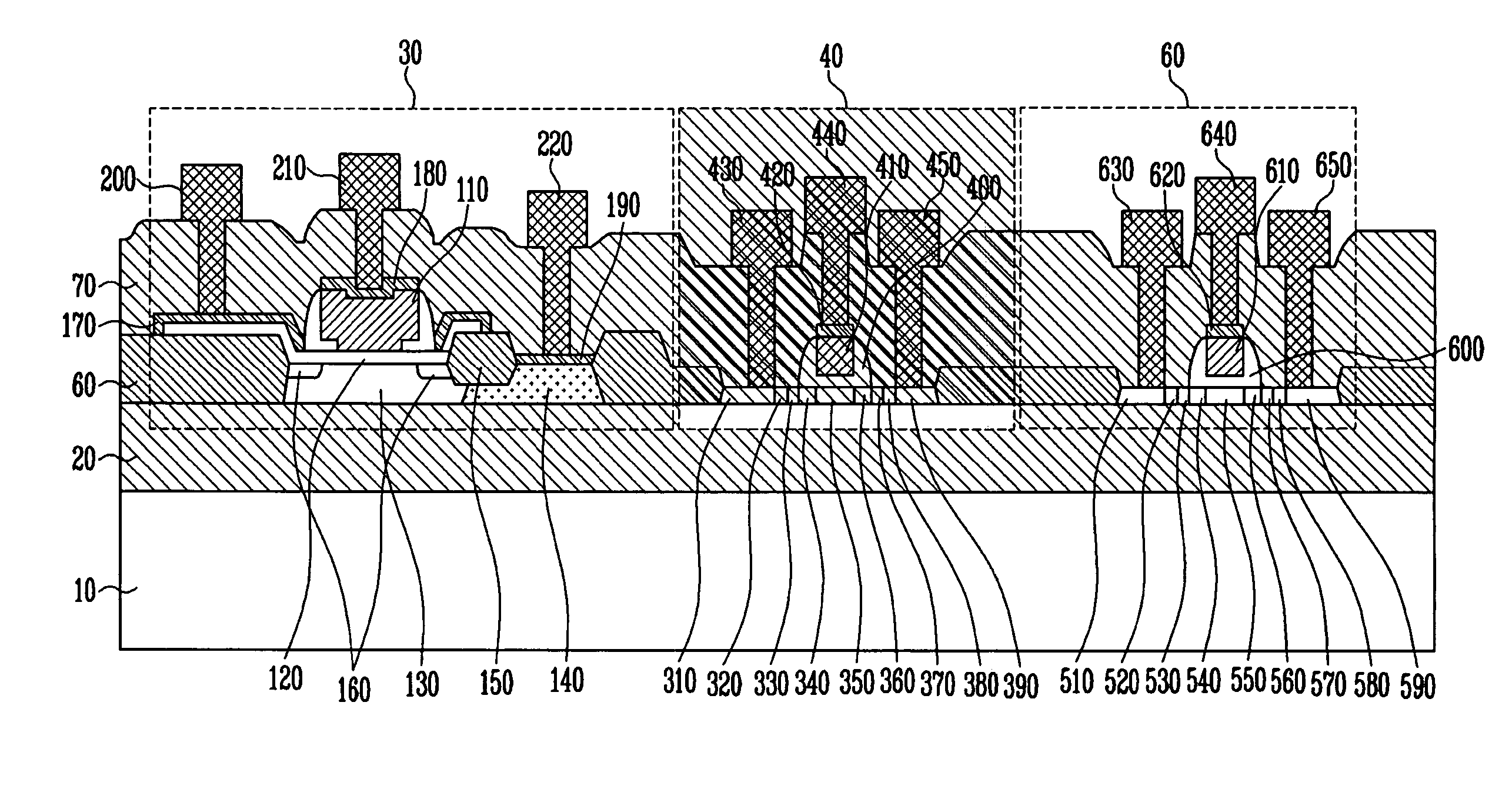
[0022]FIG. 1 is a cross-sectional view schematically illustrating a SiGe BiCMOS device according to a preferred embodiment of the present invention.

[0023] Referring to FIG. 1, the SiGe BiCMOS device includes a substrate 10, an insulating layer 20, a SiGe HBT 30, an NMOS device 40, a PMOS device 50, and a field insulating layer 60.

[0024] The substrate 10 is preferably a p-type semiconductor having a resistivity of 6 to 100Ω·cm. A high resistance substrate is a substrate which is doped at a low concentration and has good performance due to small substrate capacitance, but its price is high.

[0025] The insulating layer 20 is an oxide layer having a thickness ...


PUM


Abstract

Provided are an NMOS device, a PMOS device and a SiGe HBT device which are implemented on an SOI substrate and a method of fabricating the same. In manufacturing a Si-based high speed device, a SiGe HBT and a CMOS are mounted on a single SOI substrate. In particular, a source and a drain of the CMOS are formed of SiGe and metal, and thus leakage current is prevented and low power consumption is achieved. Also, heat generation in a chip is suppressed, and a wide operation range may be obtained even at a low voltage.

Description

CROSS-REFERENCE TO RELATED APPLICATION [0001] This application claims priority to and the benefit of Korean Patent Application No. 2003-97051, filed on Dec. 26, 2003, the disclosure of which is incorporated herein by reference in its entirety. BACKGROUND [0002] 1. Field of the Invention [0003] The present invention relates to an NMOS device, a PMOS device and a SiGe HBT device and a method of fabricating the same and, more particularly, to an NMOS device, a PMOS device and a SiGe HBT device which are integrated on a silicon on insulator (SOI) and a method of fabricating the same [0004] 2. Discussion of Related Art [0005] Typically, gallium arsenide (GaAs)-based compound semiconductors have been employed in fabricating radio frequency (RF) devices for information communication, and complementary metal oxide semiconductor (CMOS) devices have been employed in fabricating analog / digital circuits. Currently, a RF / analog / digital system-on-chip (SoC) is widely being used, and a silicon ger...

Claims


Application Information

Patent Timeline
Patent Type & Authority Applications(United States)
IPC IPC(8): H01L27/092H01L21/331H01L21/8228H01L21/84H01L27/12
CPCH01L21/84H01L29/66242H01L27/1203H01L21/8228H01L27/092H01L27/12
Inventor KANG, JIN YEONGLEE, SEUNG YUNCHO, KYOUNG IK
Owner ELECTRONICS & TELECOMM RES INST
Why Eureka
Try Eureka