Solid-state image pickup device

a solid-state image and pickup device technology, applied in the direction of color television, television system, radio control device, etc., can solve the problems of difficult microminiaturization of the device, unavoidable decrease of the amount of electric charge to be handled, and inability to main a desired dynamic range, etc., to suppress the occurrence of dark current and white spot, increase the amount of electric charge, and shallow trench isolation layer

Inactive Publication Date: 2005-06-30
SONY CORP
View PDF0 Cites 21 Cited by
  • Summary
  • Abstract
  • Description
  • Claims
  • Application Information

AI Technical Summary

Benefits of technology

[0044] As a result, since the shallow trench isolation layer includes the lower narrow portion and it is located behind the light-receiving sensor portion as compared with the related-art single shallow trench isolation layer structure, the area of the first conductivity type electric charge accumulation region of the light-receiving sensor portion can increase to increase an amount of electric charges that can be handled by the light-receiving sensor portion.
[0045] Also, a dark current generated from the side wall of the lower portion of the shallow trench isolation layer can be decreased by the second conductivity type semiconductor region formed around the lower narrow portion of the shallow trench isolation layer. In particular, the depletion layer extending from the first conductivity type electric charge accumulation region of the light-receiving sensor portion to the lateral direction is blocked by the second conductivity type semiconductor region, whereby the depletion layer can be prevented from reaching the side wall of the shallow trench isolation layer. As a consequence, it is possible to suppress the occurrence of a dark current and a white spot.
[0046] As described above, according to the present invention, since the area of the electric charge accumulation region of the photodiode of the light-receiving sensor portion can be increased as compared with the related-art single trench isolation layer stru

Problems solved by technology

Then, when the pixel portion uses the shallow trench isolation structure as described above, since a depletion layer extending from a light-receiving sensor portion reaches the side wall of the shallow trench isolation layer, there arises a problem, in which a dark current is generated at the SiO2/Si interface of the side surface of this shallow trench isolation layer.
Hence, it becomes difficult to main a desired dynamic range.
As a result, the amount of the signal electric charge that can be accumulated in the N-type semiconductor region 53 of the light-receiving sensor portion (amount of electric charges to be handled) is decreased unavoidably.
Accordingly, it is frequently observed that the widt

Method used


Image

  • Solid-state image pickup device
  • Solid-state image pickup device
  • Solid-state image pickup device

Examples


Embodiment Construction

[0054] The present invention will now be described with reference to the drawings.

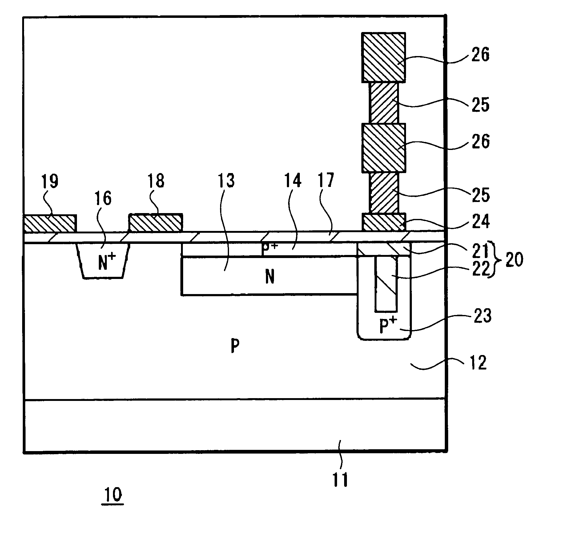
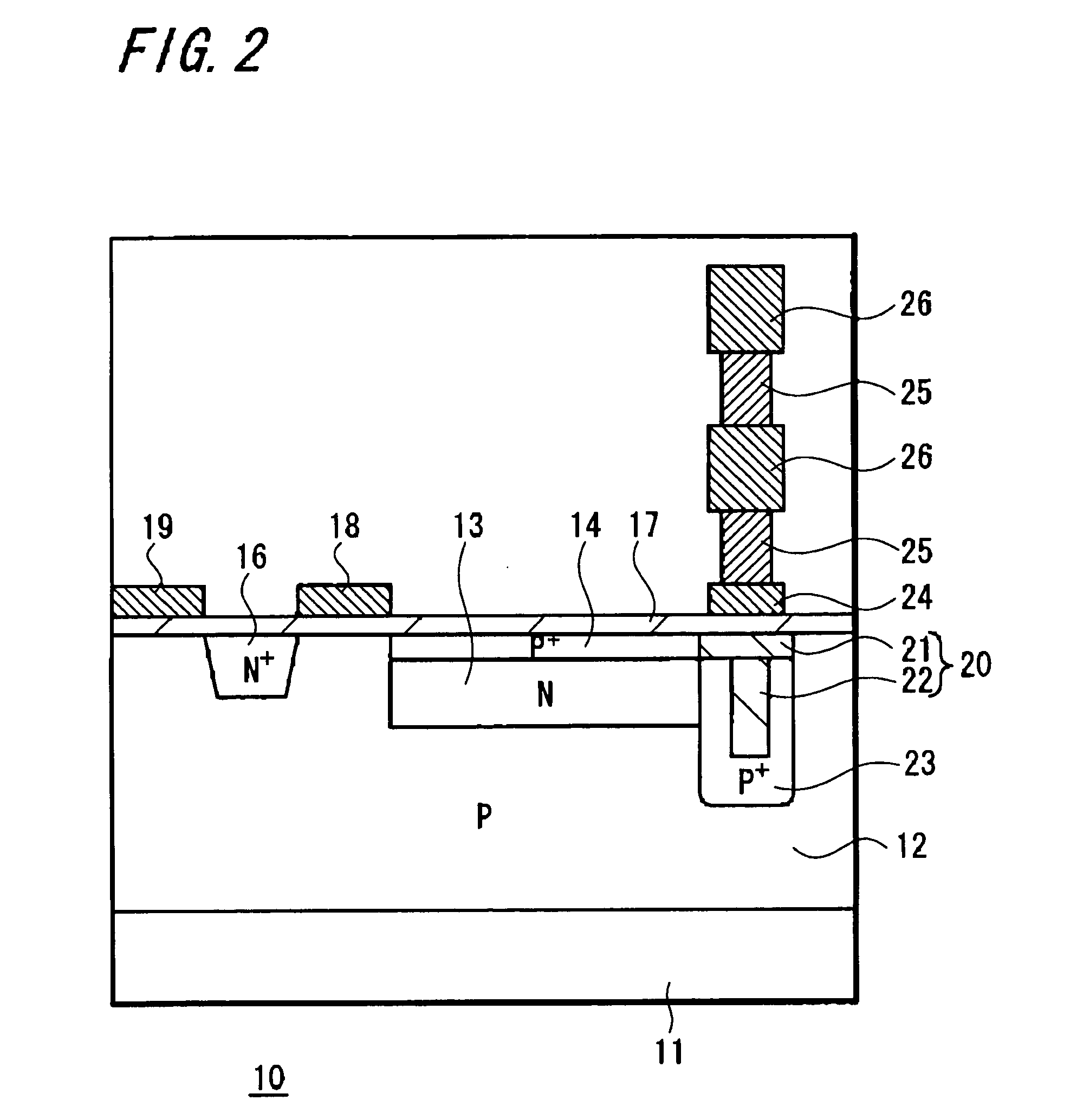
[0055]FIG. 2 is a schematic cross-sectional view showing an arrangement of a solid-state image pickup device according to an embodiment of the present invention. FIG. 2 shows a cross-section of one pixel cell. In this embodiment, the present invention is applied to a CMOS sensor (CMOS type solid-state image pickup device).

[0056] As shown in FIG. 2, a P-type semiconductor well region 12 is formed on a substrate 11, and an N-type semiconductor region 13 serving as an electric charge accumulation region of a light-receiving sensor portion and an N+ floating diffusion region 16 are formed on this P-type semiconductor well region 12.

[0057] Also, a P-type (P+) positive electric charge accumulation region 14 is formed near the surface of the substrate 11 on the N-type semiconductor well region 13.

[0058] These P-type semiconductor well region 12, N-type semiconductor well region 13 and P-type positive elec...


PUM


Abstract

A solid-state image pickup device 10 has an arrangement in which a second conductivity type semiconductor region 14 is formed on the surface of a first conductivity type electric charge accumulation region 13 of a light-receiving sensor portion, a shallow trench isolation layer 20 formed of an insulating layer is buried into a trench formed on a semiconductor substrate 11, the shallow trench isolation layer 20 is composed of an upper wide portion 21 and a lower narrow portion 22 and a second conductivity type semiconductor region 23 is formed around the lower narrow portion 22 of the shallow trench isolation layer 20. The solid-state image pickup device can suppress the occurrence of a dark current and a white spot, it can produce an image with high image quality and it can sufficiently maintain a sufficiently large amount of electric charges that can be handled by the light-receiving sensor portion.

Description

BACKGROUND OF THE INVENTION [0001] 1. Field of the Invention [0002] The present invention relates to a solid-state image pickup device. [0003] 2. Description of the Related Art [0004] As a pixel cell of a solid-state image pickup device becomes micro-miniaturized more, particularly in a CMOS (complementary metal-oxide semiconductor) sensor (CMOS type solid-state image pickup device), it is frequently observed that a pixel portion also uses a trench element isolation structure (so-called STI : shallow trench isolation) structure similarly to a peripheral circuit portion. [0005] Also, it becomes customary that a light-receiving portion uses a buried photodiode structure to decrease a dark current. [0006] Then, when the pixel portion uses the shallow trench isolation structure as described above, since a depletion layer extending from a light-receiving sensor portion reaches the side wall of the shallow trench isolation layer, there arises a problem, in which a dark current is generate...

Claims


Application Information

Patent Timeline
IPC IPC(8): H01L27/146H01L27/14H01L27/148H01L31/00H01L31/10H04N5/335H04N5/361H04N5/367H04N5/369H04N5/374
CPCH01L27/1463H01L27/14689H01L27/14643H01L27/148H01L31/10
Inventor KANBE, HIDEO
Owner SONY CORP
Why Eureka
Try Eureka