Diode laser subelement and arrangements with such diode laser subelement

a diode laser and subelement technology, applied in lasers, semiconductor laser arrangements, laser construction details, etc., can solve problems such as unsatisfactory address, disadvantageous mounting complexity, and high production complexity, and achieve the effect of low production complexity

Inactive Publication Date: 2005-06-30
LORENZEN DIRK
View PDF11 Cites 30 Cited by
  • Summary
  • Abstract
  • Description
  • Claims
  • Application Information

AI Technical Summary

Benefits of technology

[0013] Starting at this point, it is the object of the invention to connect the expansion-adapted mounting and the electrical contacting of laser diode elements to one another in terms of structural engineering such that the laser diode elements can be stacked and / or arranged laterally in one plane with low production complexity for producing vertical diode laser arrangements.

Problems solved by technology

Thus there are two joint zones situated between the secondary heat elimination side-electrical feed line, above and below the electrical insulation stratum, which means disadvantageous mounting complexity.
Another disadvantage in known diode lasers relates to providing connection options for electrical contact elements for the electrical supply of the laser diode bar via power cable.
In both cases a contact or joint zone occurs that involves disadvantageous mounting complexity.
Another unsatisfactorily addressed object relates to the modular integration of diode laser elements or diode lasers in arrangements of a plurality of diode laser elements or diode lasers.
While series connection of the diode laser elements is realized in a simple manner in these vertical diode laser arrangements in that the strip conductor, attached to the laser diode bar on the secondary heat elimination side, of a first diode laser element is in direct or indirect electrical contact with the heatsink as a main heat elimination side-electrical contact of a second diode laser component located thereabove, for lateral diode laser arrangements there is the problem of converting the vertical electrical contact element arrangement into a series connection of the diode laser elements that can be arranged laterally.

Method used


Image

  • Diode laser subelement and arrangements with such diode laser subelement
  • Diode laser subelement and arrangements with such diode laser subelement
  • Diode laser subelement and arrangements with such diode laser subelement

Examples


Embodiment Construction

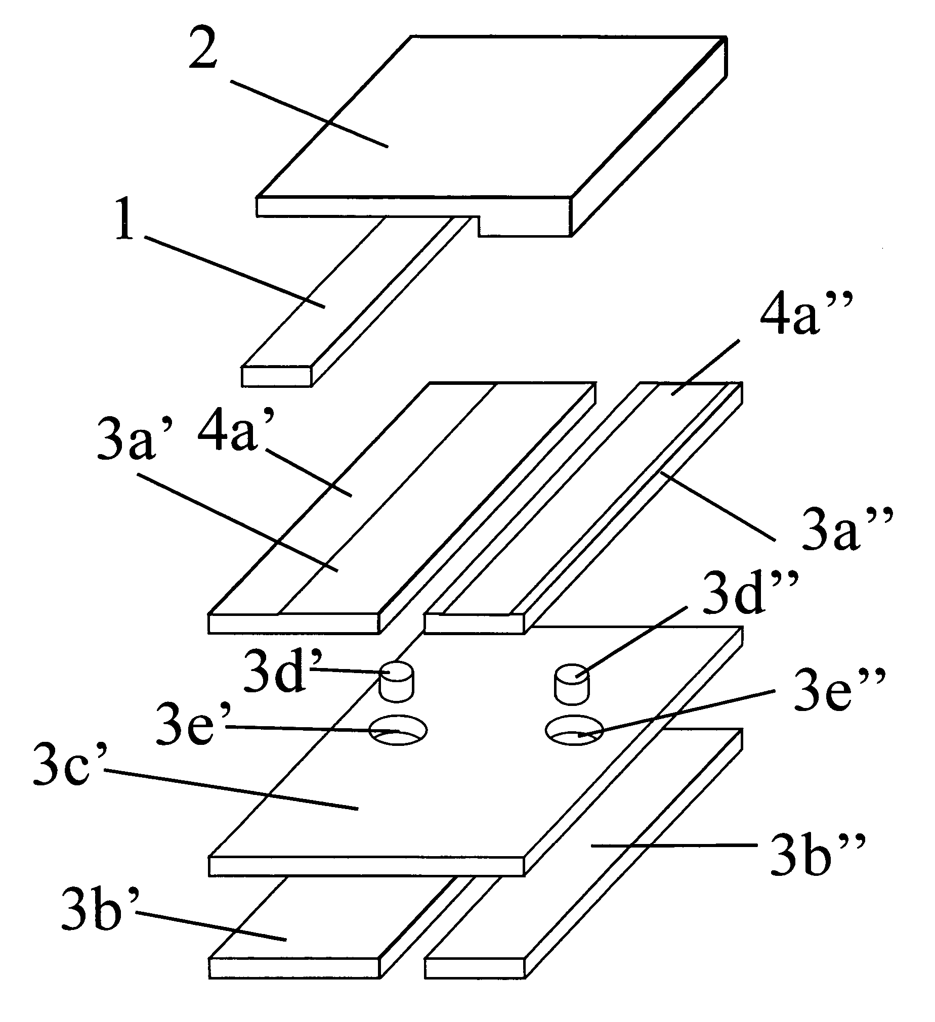
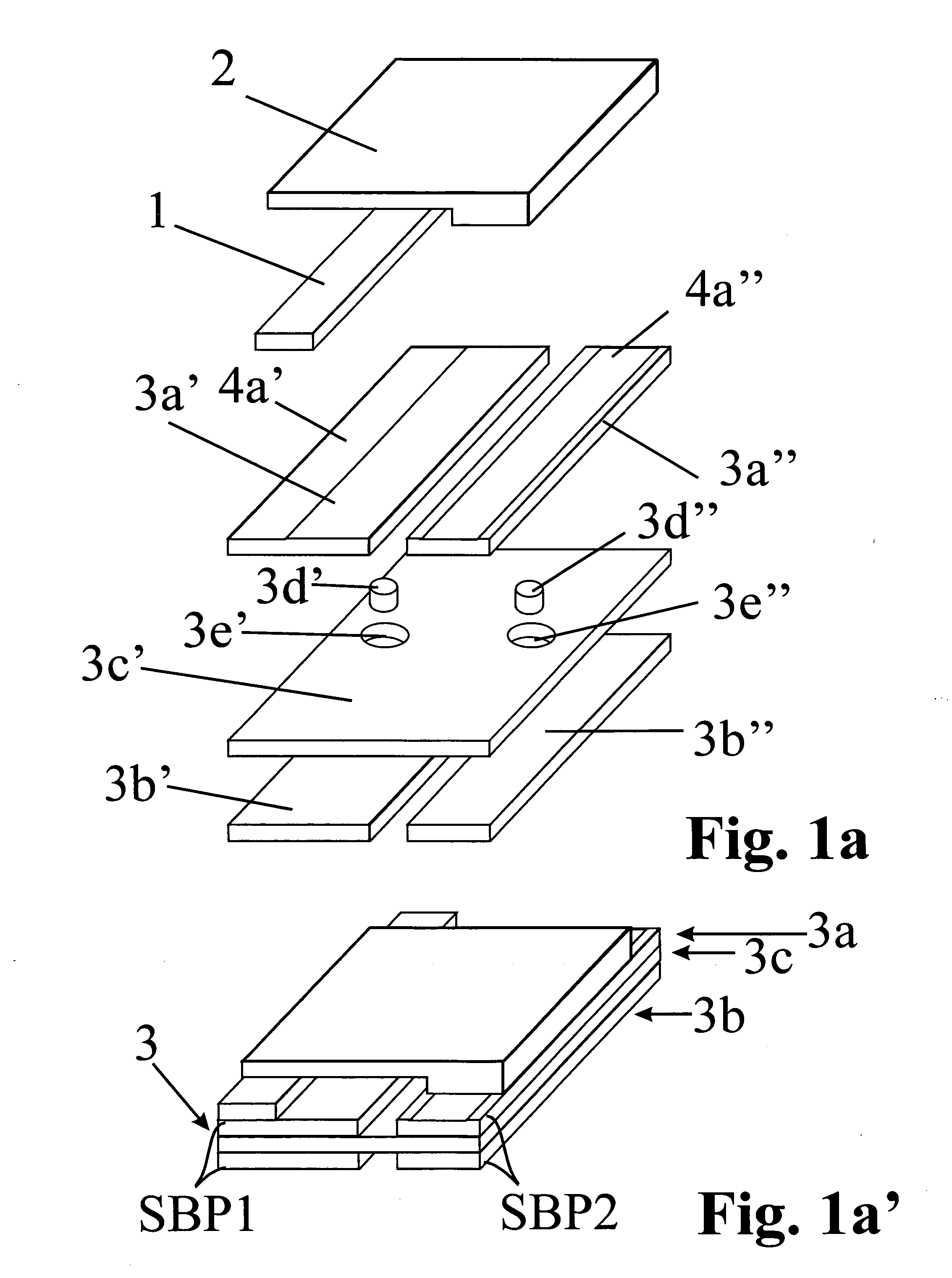
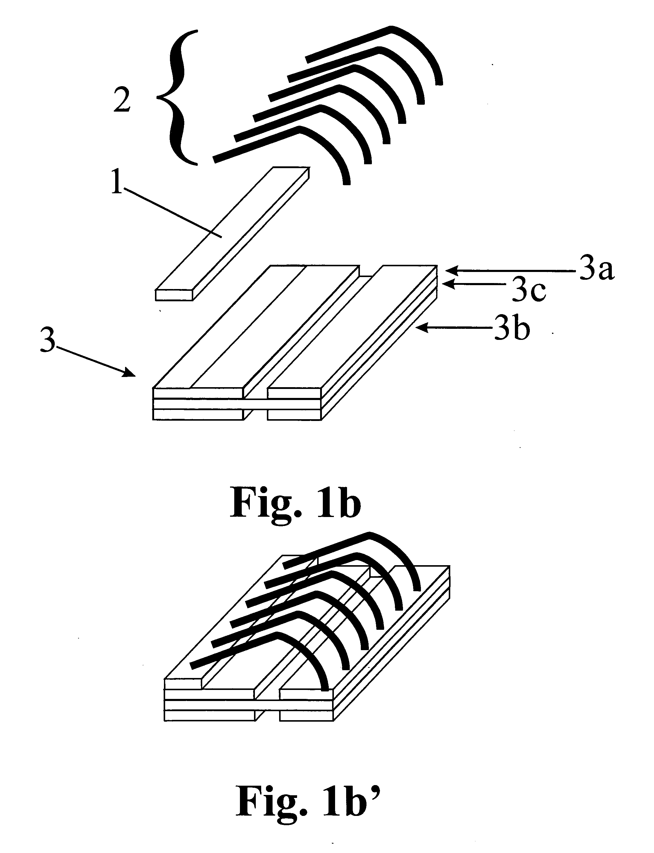
[0043] The diode laser subelement B illustrated in FIGS. 1a and 1′ includes a laser diode element 1 embodied as laser diode bars, an electrically conductive connecting element 2 (metallic film), a multilayer substrate 3 that is constructed of at least three layers materially joined to one another, an upper layer 3a that is provided for mounting the laser diode element 1 and is therefore exposed, a lower layer 3b adjunct to the upper layer, and a separating layer 3c interposed therebetween. The electrically conducting connecting element 2 in this embodiment is produced from one piece, including a step for height equalization in the electrical contacting of the laser diode element 1.

[0044] The upper exposed and the lower adjunct layer 3a, 3b contain first and second metallic strata regions 3a′, 3a″, 3b′ and 3b″ arranged spaced from one another that are electrically separated from one another on each layer 3a, 3b, of which however for forming strata region pairs SBP 1 and SBP 2 each s...


PUM


Abstract

Expansion-adapted mounting and electrical contacting of laser diode elements are connected with one another in terms of structural engineering such that the laser diode elements can be stacked or arranged laterally in one plane for producing vertical diode laser arrangements with low production complexity. The upper and the lower layers of a heat-distributing multilayer substrate for a diode laser subelement, between which a separating layer is disposed, contain metal strata regions arranged spaced from one another of which for forming strata region pairs each strata region of the upper layer is joined electrically conducting to a strata region of the lower layer. The separating layer contains at least one electrically insulating stratum made of non-metallic material and the sum of the thicknesses of metallic strata in the multilayer substrate exceeds the sum of the thicknesses of non-metallic strata at least in a partial region perpendicular to the mounting surface for at least one laser diode element.

Description

BACKGROUND OF THE INVENTION [0001] The invention relates to a diode laser subelement with at least one laser diode element applied to a mounting surface of a heat-distributing multilayer substrate, whereby the multilayer substrate is joined materially with one another, made of an upper, a lower, and at least one separating layer interposed therebetween. [0002] Laser diode elements include individual laser diodes and laser diode bars. Individual laser diodes have only a single laser diode emitter that is defined by an optically continuous active area. Laser diode bars are monolithic semiconductor laser arrangements of at least two operational laser diode emitters that are optically largely independent of one another. The lateral reach of laser diode bars is a factor of the width, spacing, and number of emitters. Typical widths are in the range of 1 to 15 mm. [0003] For reliable operation as a diode laser, the laser diode elements are mounted on a heatsink that distributes, and, in th...

Claims


Application Information

Patent Timeline
Patent Type & Authority Applications(United States)
IPC IPC(8): H01S3/04H01S5/022H01S5/024H01S5/40
CPCH01S5/02264H01S5/02272H01S5/02276H01L2224/49175H01S5/4018H01S5/4025H01S5/405H01S5/02423H01S5/02365H01S5/0237H01S5/02345
Inventor LORENZEN, DIRK
Owner LORENZEN DIRK
Why Eureka
Try Eureka