Chemical-mechanical planarization controller

a controller and chemical technology, applied in the field of chemical-mechanical planarization, can solve the problems of limiting the kind of system performance that can be achieved, and achieve the effects of reducing the dynamic model of control, superior control performance, and maximum performan

Active Publication Date: 2005-06-30
SOLUTIONS
View PDF3 Cites 17 Cited by
  • Summary
  • Abstract
  • Description
  • Claims
  • Application Information

AI Technical Summary

Problems solved by technology

Traditional single-input single-output design approaches would limit the kind of performance that can be achieved in systems with strong coupling between various input and / or output variables.

Method used


Image

  • Chemical-mechanical planarization controller
  • Chemical-mechanical planarization controller
  • Chemical-mechanical planarization controller

Examples


Embodiment Construction

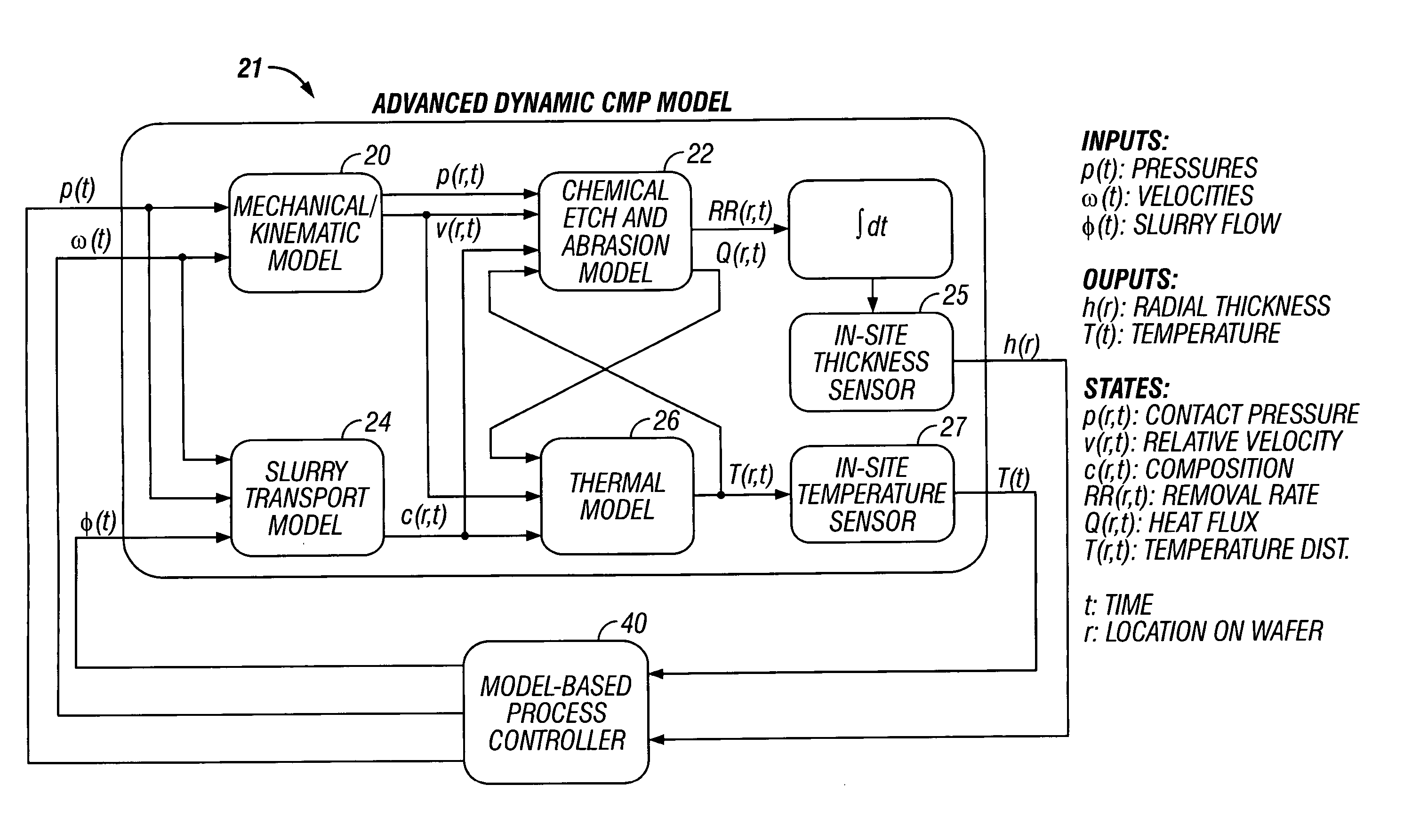
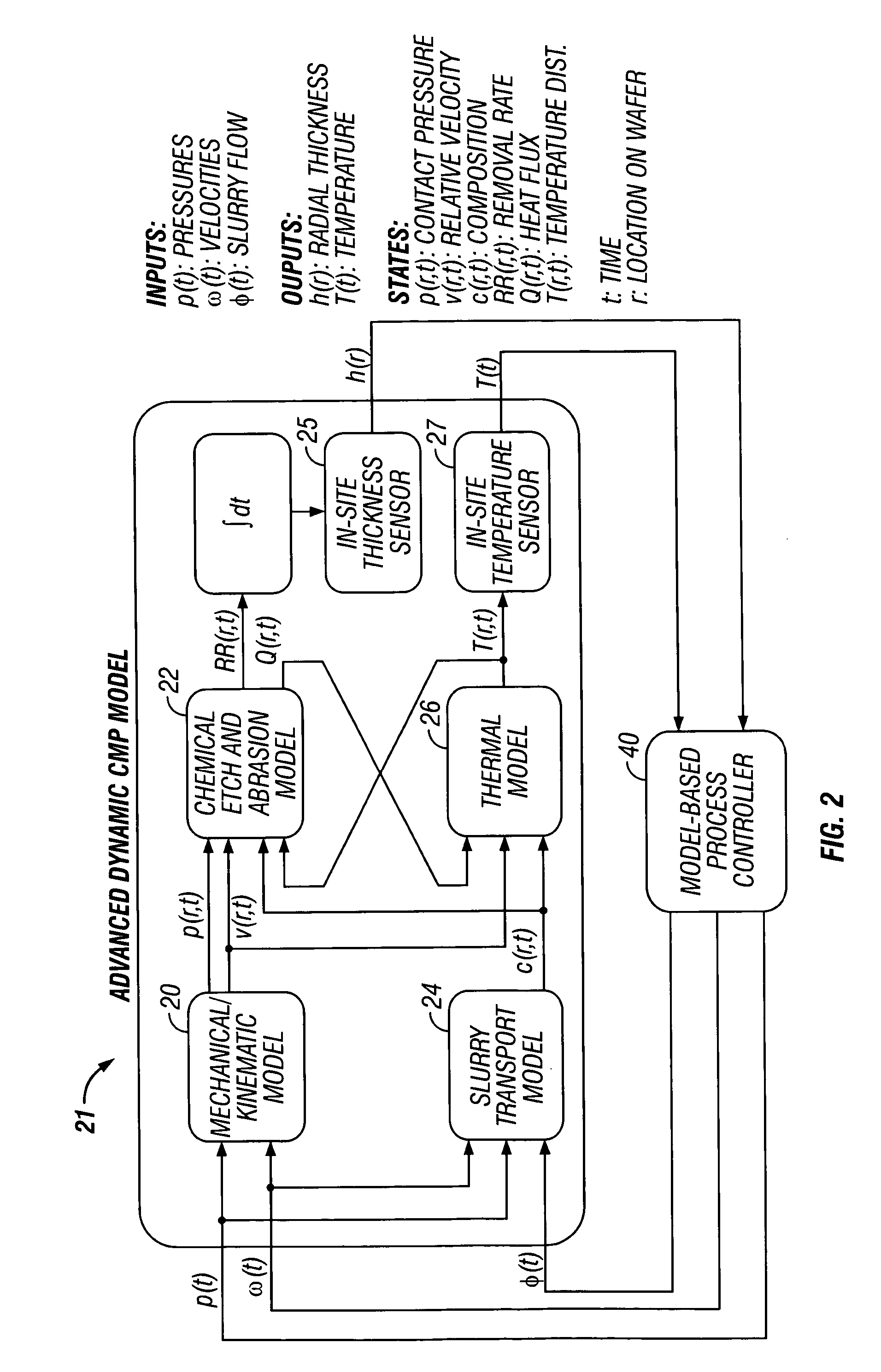
In-Situ Sensing (25, 27)

[0028] A recent development in CMP is the use of real-time in-situ sensors, such as optical or optical-eddy-current sensors 25 to monitor wafer-scale as well as die-scale uniformity, and allow real-time feedback control of wafer uniformity. The primary objective is to control global planarity. Therefore, it is necessary to sense variations (non-uniformity) in the removal rate at the wafer-scale as well as die-scale. Off-line metrology can be used to monitor both wafer as well as die-scale uniformity, and the resulting measurements can be used for run-to-run control. Several sensors have been proposed for and used in CMP for monitoring the material removal rate. See M. Sun, H.-M. Tzeng, H. Litvak, D. Glenn, In-situ Detection of Film Thickness Removal During CMP of Oxide and Metal Layers, Proc. CMP-MIC, February 1996; S. Inaba, et. al., Study of CMP Polishing Pad Control Method, CMP-MIC Conference, 1998 IMIC-300P / 98 / 0044, pp. 44-51, 1998; KLA-Tencor, Press Re...


PUM


Abstract

The invention provides a model-based control approach to chemical-mechanical planarization (CMP) control. The preferred embodiment comprises mathematical models of the CMP process. These models play a critical role in obtaining superior control performance. Model-based Control Design involves the construction of a dynamic mathematical model of the system to be controlled, e.g. a removal rate model of a CMP system. The model can then be evaluated via computer simulations, and validated using data from the system. The invention provides a method and apparatus that processes in-situ data from a suite of real-time sensors and produces real-time commands to multiple actuators, such as applied pressures, slurry-flow rate, and wafer / pad velocity. A key aspect of the invention is an integrated model-based pressure-temperature-velocity-slurry flow control system that includes many innovations in real-time mode identification, real-time gain estimation, and real-time control.

Description

BACKGROUND OF THE INVENTION [0001] 1. Technical Field [0002] The invention relates to chemical-mechanical planarization. More particularly, the invention relates to a chemical-mechanical planarization controller. [0003] 2. Description of the Prior Art [0004] Chemical-Mechanical Planarization (CMP) is an important step in the processing of semiconductor wafers and is playing an increasingly critical role in semiconductor microelectronics fabrication (see The National Technology Roadmap for Semiconductors, Semiconductor Industry Association, San Jose, Calif. 1997; J. M. Steigerwald, S. P. Murarka, R. J. Gutman, Chemical Mechanical Planarization of Microelectronic Materials, Wiley Interscience, 1997; and W. J. Patrick, W. L. Guthrie, C. L. Stanley, and P. M. Schiable, Application of Chemical Mechanical Polishing to the Fabrication of VLSI Circuit Interconnection, J. Electrochem. Soc., 138,1778-1784, 1991). [0005] CMP is a process for material removal that uses chemical and mechanical a...

Claims


Application Information

Patent Timeline
Patent Type & Authority Applications(United States)
IPC IPC(8): G05B17/02G06F19/00
CPCG05B17/02G05B2219/45232G05B2219/32342Y02P90/02
Inventor ROOVER, DIRK DEEMAMI-NAEINI, ABBASEBERT, JON LLOYD
Owner SOLUTIONS
Why Eureka
Try Eureka