MRAM having error correction code circuitry and method therefor

a random access memory and error correction technology, applied in the field of magnetic random access memories, can solve the problems of poor write endurance of flash memory, high voltage requirements, slow program and erase times,

Active Publication Date: 2005-06-30
EVERSPIN TECHNOLOGIES
View PDF8 Cites 43 Cited by
  • Summary
  • Abstract
  • Description
  • Claims
  • Application Information

AI Technical Summary

Problems solved by technology

Disadvantages of FLASH memory include high voltage requirements and slow program and erase times. Also, FLASH memory has a poor write endurance of 104-106 cycles before memory failure.
Hence, FLASH memory is limited in the dimensions to which it can be scaled.
As the lateral dimension of an MRAM device decreases, several problems occur.
First, the switching field increases for a given shape and film thickness, requiring a larger magnetic field to switch.
The energy b...

Method used


Image

  • MRAM having error correction code circuitry and method therefor
  • MRAM having error correction code circuitry and method therefor
  • MRAM having error correction code circuitry and method therefor

Examples


Embodiment Construction

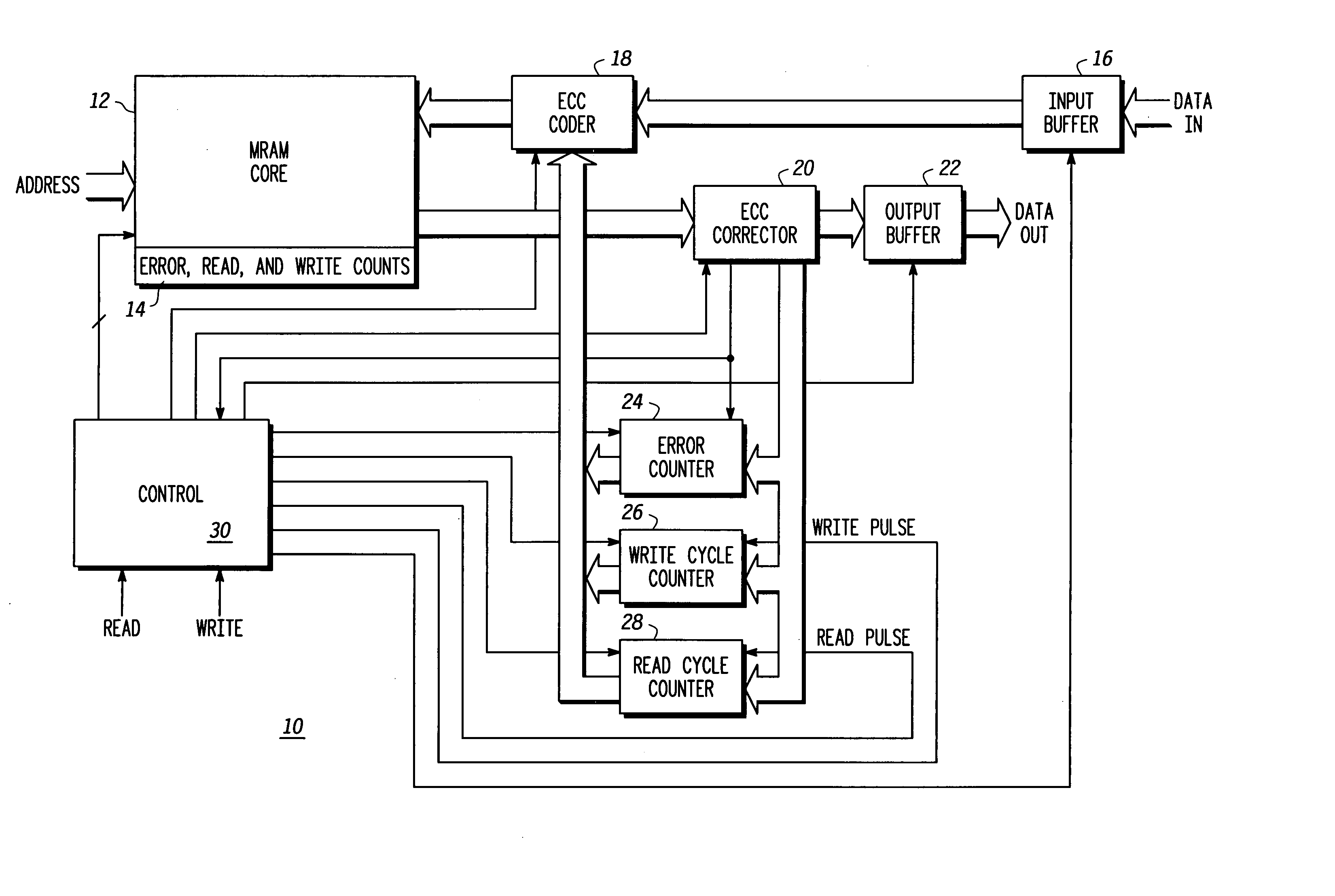
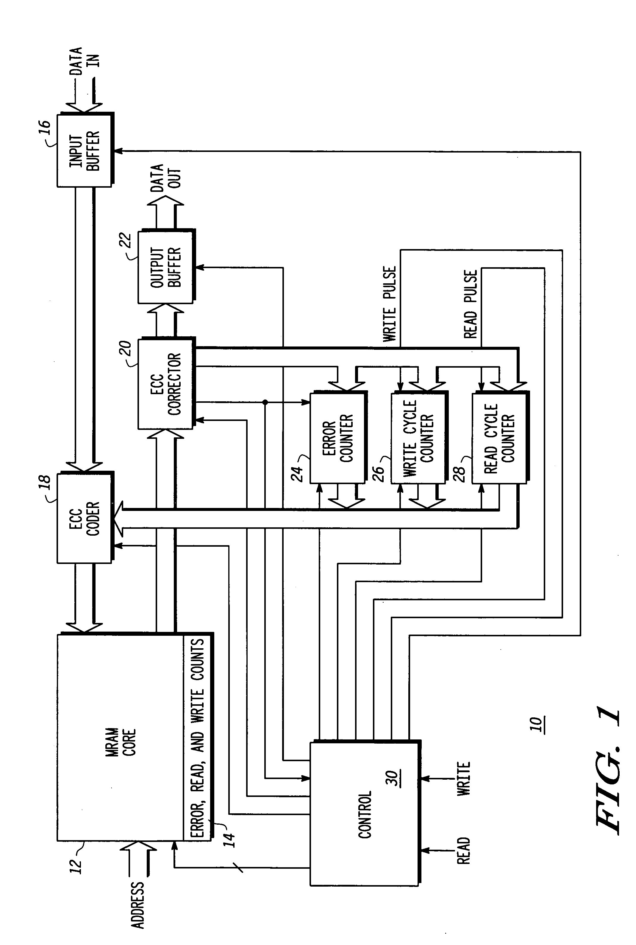
[0011]FIG. 1 illustrates an embedded memory system 10 having error correction circuitry with a counter for counting detected errors during normal read and write cycle operation. An MRAM core 12 is generally illustrated. It should be understood that the MRAM core 12 contains column and row decoders, read sense amplifiers and write drivers that are not specifically illustrated. The MRAM is accessed by an address bus that receives an address value labeled “Address”. The MRAM core 12 also has an error, read and write counts field 14 that is a special memory location for storing error counts, read cycle counts and write cycle counts.

[0012] An input buffer 16 has an input coupled to a bus for receiving input data labeled “Data In”. An output of the input buffer 16 is connected via a bus to an input of an Error Correction Code (ECC) coder 18. An output of the ECC coder 18 is connected to a data input of the MRAM core 12 via a bus. A data output of the MRAM core 12 is connected via a bus t...


PUM


Abstract

An embedded memory system (10) uses an MRAM core (12) and error correction code (ECC) corrector circuitry (20). The ECC corrector circuitry identifies soft memory bit errors which are errors primarily resulting from an MRAM bit not being correctly programmed. The errors are identified and corrected during a read or a write cycle and not necessarily when the memory is in a special test mode. As errors are corrected, the error corrections are counted by an error counter (24) to create a count value. The count value is stored in the MRAM core itself and can later be retrieved and read during a test mode for an indication of how many bit corrections are required for the MRAM core over a period of time. The count value is stored by using an unused portion of a write memory cycle during a read operation.

Description

FIELD OF THE INVENTION [0001] This invention relates to Magnetoresistive Random Access Memories (MRAMs), and more particularly to reliability of operation of MRAMs. BACKGROUND OF THE INVENTION [0002] Non-volatile memory devices, such as FLASH memories, are extremely important components in electronic systems. FLASH is a major non-volatile memory device in use today. Disadvantages of FLASH memory include high voltage requirements and slow program and erase times. Also, FLASH memory has a poor write endurance of 104-106 cycles before memory failure. In addition, to maintain reasonable data retention, the scaling of the gate oxide is restricted by the tunneling barrier seen by the electrons. Hence, FLASH memory is limited in the dimensions to which it can be scaled. [0003] To overcome these shortcomings, magnetic memory devices are being evaluated. One such device is magnetoresistive random access memory (hereinafter referred to as “MRAM”). To be commercially practical, however, MRAM m...

Claims


Application Information

Patent Timeline
IPC IPC(8): G06F11/10G11C29/00G11C29/42G11C29/44
CPCG06F11/1008G11C11/16G11C29/42G06F2211/109G11C2029/1208G11C2029/4402G11C29/44
Inventor NAHAS, JOSEPH J.
Owner EVERSPIN TECHNOLOGIES
Why Eureka
Try Eureka