Discrete and integrated photo voltaic solar cells

a solar cell and photovoltaic technology, applied in the field of solar cells, can solve the problems of high degree of defects, high material and labor costs, and high cost of di technology, and achieve the effect of high efficiency

Active Publication Date: 2005-07-07
LITTELFUSE INC
View PDF19 Cites 62 Cited by
  • Summary
  • Abstract
  • Description
  • Claims
  • Application Information

AI Technical Summary

Benefits of technology

[0011] By using microelectronic techniques disclosed herein, the resultant PV device that outputs a high voltage (e.g., 3 volts) is made much smaller than a conventional device that outputs comparable voltage (see FIG. 1B). In the present embodiment, a relatively small die sized PV device can be packaged in simple packages, like the ones used in discrete semiconductor devices, e.g., LEDs, transistor diodes etc., with a transparent plastic encapsulation.
[0012] As used herein, a packaged device including a PV die is referred to as a “packaged PV device.” The packaged PV device may include one or more PV dice as well as other components. As used herein, a “PV device” generally refers to a die including one or more solar cells. However, PV device may also refer to a packaged PV device, particularly when used in the claims.
[0013] In one embodiment, a packaged PV device has a plurality of pins, e.g., two pins, and can be used as a discrete component in a desired circuit or product. Such a discrete product (or a single packaged product) contains one or more small, packaged PV devices with high voltage outputs. Each PV device or die generates about 0.6-0.7 volt of output. The discrete product enables the operation of portable electronic ...

Problems solved by technology

This results in increased material and labor costs.
The DI technology is costly and is generally considered to be impractical.
This technology, as explained above, requires deposition of a thick layer of polysilicon and ...

Method used


Image

  • Discrete and integrated photo voltaic solar cells
  • Discrete and integrated photo voltaic solar cells
  • Discrete and integrated photo voltaic solar cells

Examples


Embodiment Construction

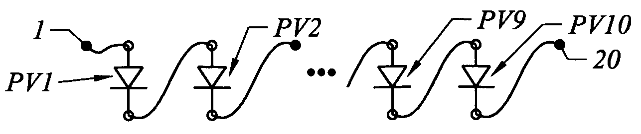
[0031] The present invention relates to photo voltaic solar cells. For part of the reasons described above in the background, embodiments of the present invention provide a structure and a method of making a PV chip that can provide a high voltage output by integrating multiple single PV solar cell diodes in one monolithic substrate, e.g., silicon substrate or crystal.

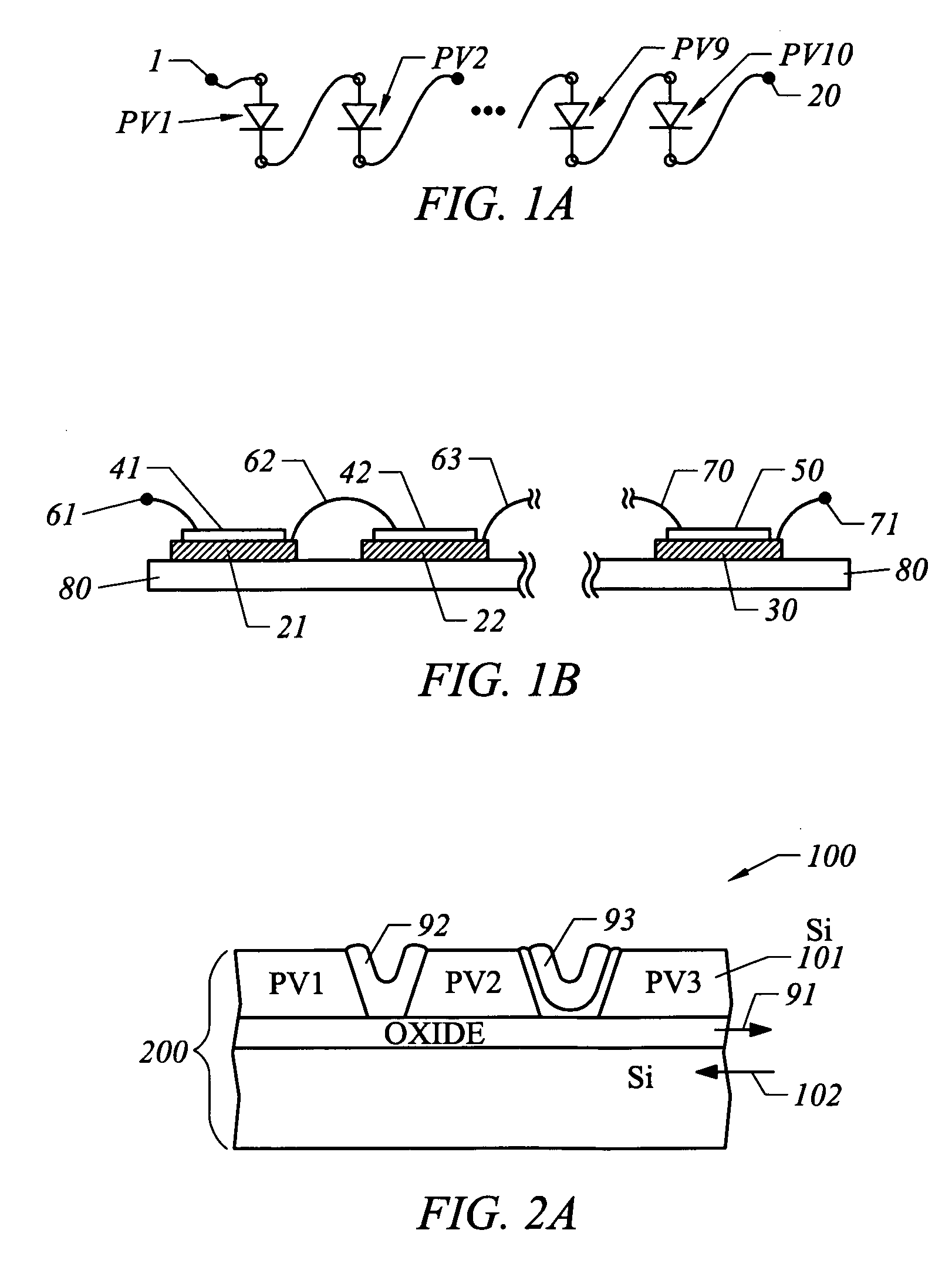
[0032]FIG. 2A illustrates a cross-sectional view of a discrete PV device or die 100 according to one embodiment. The PV device 100 is formed using an SOI (Silicon on Insulator) technique to fabricate high efficiency PV cell arrays on a single semiconductor die. The die is packaged as a single discrete device. The PV device includes a first silicon substrate 101 and a second silicon substrate 102. At least one of the two substrates is thermally oxidized to form a silicon dioxide layer 91. The two substrates are bonded together by sandwiching the silicon dioxide layer between them. This creates a bonded structure 200. T...


PUM


Abstract

A photovoltaic (PV) cell device comprises a first semiconductor substrate; a second semiconductor substrate bonded to the first semiconductor substrate; an insulating layer provided between the first and second substrates to electrically isolate the first substrate from the second substrate; a plurality of PV cells defined on the first substrate, each PV cell including a n-type region and a p-type region; a plurality of vertical trenches provided in the first substrate to separated the PV cells, the vertical trenches terminating at the insulating layer; a plurality of isolation structures provided within the vertical trenches, each isolation structure including a first isolation layer including oxide and a second isolation layer including polysilicon; and an interconnect layer patterned to connect the PV cells to provide X number of PV cells in series and Y number of PV cells in parallel. The n-type regions are formed by performing ion implantation of arsenic to provide shallow junction depths for the n-type regions, so that PV cell device is optimized for sunlight.

Description

CROSS REFERENCES TO RELATED APPLICATIONS [0001] The present application claims priority from U.S. Provisional Patent Application No. 60 / 508,351, filed on Oct. 3, 2003, which is incorporated by reference.BACKGROUND OF THE INVENTION [0002] The present invention relates to solar cells formed on a semiconductor substrate. [0003] State of the art high efficiency photo voltaic (“PV”) solar cells have been introduced as a component in a die (chip) or wafer. A typical solar cell producer uses semiconductor manufacturing processes that are specialized to produce the PV solar cells. The same producer sells the solar cells in the form of chips or wafers. Each solar cell is formed on a single chip or wafer. The buyer of these cells then assembles them in large panels in a series or series-and-parallel combination to produce a higher output power than is possible from one monolithic solar cell. [0004] A solar cell, in its basic form, is a p / n junction (a diode) that generates 0.4-0.7 volts when ...

Claims


Application Information

Patent Timeline
IPC IPC(8): H01L27/142H01L31/00H01L31/048H01L31/05
CPCH01L31/048Y02E10/50H01L31/0508H01L31/0504H01L31/0475
Inventor POLCE, NESTORECLARK, RONALD P.ZOMMER, NATHAN
Owner LITTELFUSE INC
Why Eureka
Try Eureka