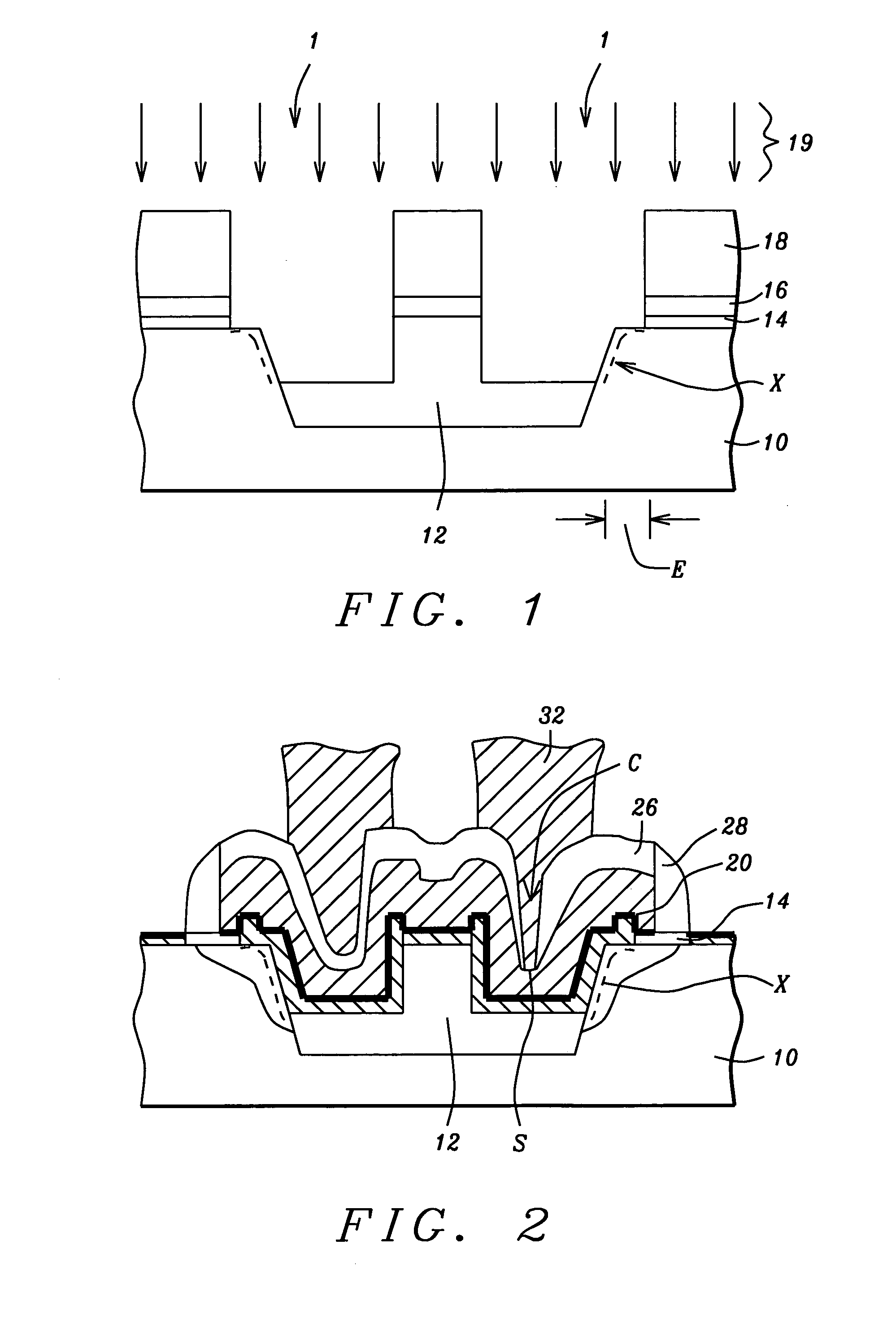
Novel random access memory (RAM) capacitor in shallow trench isolation with improved electrical isolation to overlying gate electrodes

Active Publication Date: 2005-07-14
TAIWAN SEMICON MFG CO LTD
View PDF9 Cites 16 Cited by
  • Summary
  • Abstract
  • Description
  • Claims
  • Application Information

AI Technical Summary

Benefits of technology

[0012] A further objective is to form a top electrode sufficiently thick to fill the bottle-shaped cavity and to provide a more planar surface over the restriction at the top of the bottle-shaped cavity for forming more reliable overlying gate electrodes.
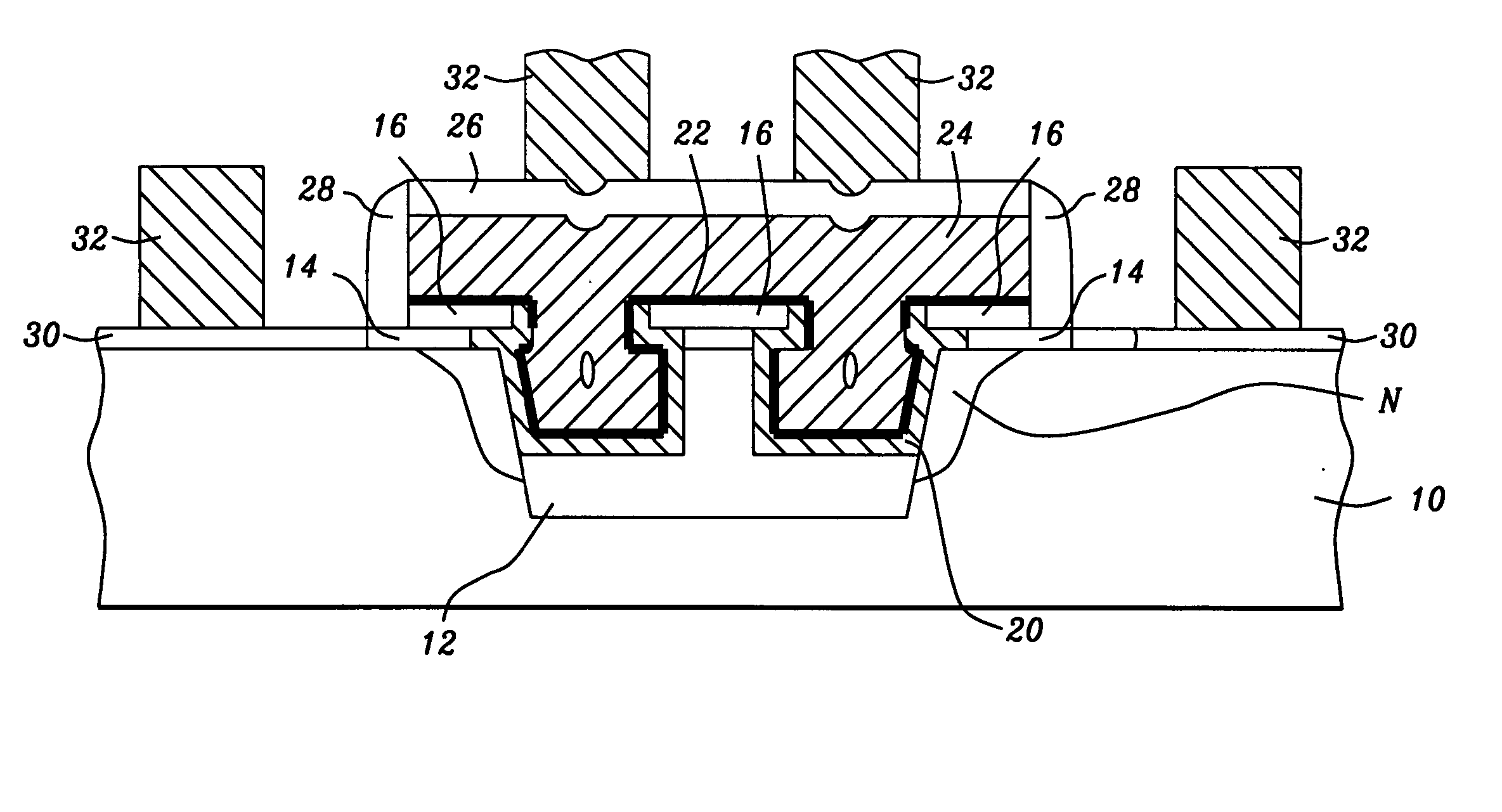
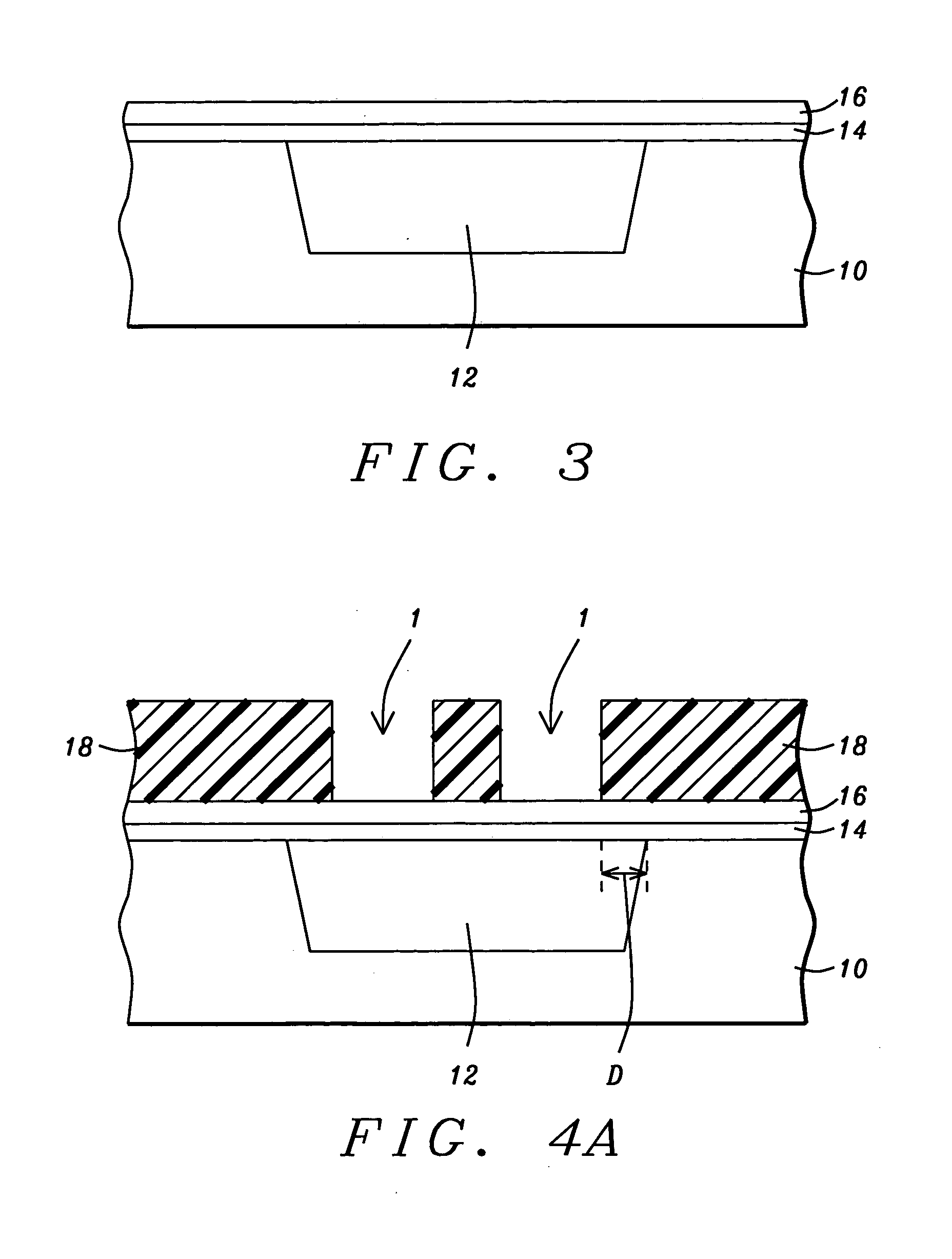
[0013] In accordance with the present invention a method for making novel recessed RAM stacked capacitor structures for 1T-SRAM-type devices with increased circuit density is described. More specifically, the method is described for making RAM capacitors in a shallow trench isolation (STI) on a substrate. The method begins by forming trenches in the substrate, filling the trenches with an insulating material to form the STI which surrounds and electrically isolates active device areas. The STI is formed planar with the top surface of the substrate. A pad oxide layer is formed on the substrate, and a first hard-mask layer is deposited on the pad oxide layer. A photoresist mask having openings is used to form recesses for capacitor bottom electrodes in the STI. A key feature is that the photoresist mask is designed to form the recesses to lie within the STI region to avoid plasma-etch damage to the active device areas. The recesses are then etched in the first hard-mask layer, in the pad oxide layer, and partially into the STI and leaving portions of the STI along edges of the active device areas to prevent plasma-etching damage to the active device areas. Anisotropic plasma etching is used during this process step. An isotropic wet etch (HF/H2O) is used to remove the exposed portions of the STI o

Problems solved by technology

However, there are several structure problems and processing problems which are described with respect to FIGS. 1 and 2.
Unfortunately, when the openings (not shown) in the photoresist mask extend over the edge of the substrate 10 (active device areas), the plasma etching, indicated by the verti

Method used


Image

  • Novel random access memory (RAM) capacitor in shallow trench isolation with improved electrical isolation to overlying gate electrodes
  • Novel random access memory (RAM) capacitor in shallow trench isolation with improved electrical isolation to overlying gate electrodes
  • Novel random access memory (RAM) capacitor in shallow trench isolation with improved electrical isolation to overlying gate electrodes

Examples


Example

[0017] The method for making these RAM capacitors in a shallow trench isolation for 1-TSRAM applications is now described in detail. These capacitor structures are made with reduced plasma-etch damage to the substrate adjacent to the STI capacitor. Also, the capacitor is designed to have a bottle-shaped structure to maximize the capacitance while providing a top electrode that is essentially planar. The planar surfac allows the word lines (gate electrodes) to extend over th capacitor for increased density while minimizing electrical shorts between the word lines and the underlying capacitor top electrodes. Although the capacitor structure is made for 1-TSRAM devices, it should be understood that this novel structure is also applicable to RAM structures in general.

[0018] Referring first to FIG. 3, the method begins by providing a substrate 10, such as a P-doped single-crystal silicon. Shallow trenches are etched in the substrate 10 to a depth of between about 2500 and 5000 Angstroms...


PUM


Abstract

A process for fabricating a novel random access memory (RAM) capacitor in a shallow trench isolation (STI). The method utilizes a novel node photoresist mask for plasma etching recesses in the STI that prevents plasma-etch-induced defects in the substrate. This novel photoresist mask is used to etch bottle-shaped recesses in the STI under a first hard mask. After forming bottom electrodes in the recesses and forming an interelectrode dielectric layer, a conducting layer is deposited sufficiently thick to fill the recesses and to form a planar surface, and a second hard mask is deposited. The conducting layer is patterned to form the capacitor top electrodes. This reduced topography results in reduced leakage currents when the gate electrodes are formed over the capacitor top electrodes.

Description

BACKGROUND OF THE INVENTION [0001] (1) Field of the Invention [0002] The present invention relates to a process for making storage capacitors for random access memory (RAM) devices, and more specifically for making improved RAM capacitors in recesses in shallow trench isolation (STI) with overlying gate electrodes for increased circuit density on 1T-SRAM cells. The 1T-SRAM cells are used in system-on-a-chip (SoC) technologies. The method of this invention utilizes a novel node photoresist mask for plasma etching recesses in the STI that prevents plasma-etch-induced defects in the substrate. This novel photoresist mask also provides bottle-shaped capacitor structures which maximizes capacitance while concurrently reducing the surface topography over the capacitor top electrodes. This reduced topography results in reduced leakage currents when the gate electrodes are formed over the capacitor top electrodes for increased circuit density. [0003] (2) Description of the Prior Art [0004] ...

Claims


Application Information

Patent Timeline
IPC IPC(8): H01L21/02H01L21/311H01L21/8242H01L27/108
CPCH01L21/31144H01L21/76237H01L21/823481H01L28/40H01L27/10861H01L27/1087H01L27/10835H10B12/377H10B12/0387H10B12/038
Inventor TU, KUO-CHI
Owner TAIWAN SEMICON MFG CO LTD
Why Eureka
Try Eureka