Scan flip flop, semiconductor device, and production method of semiconductor device

Inactive Publication Date: 2005-07-14
PANASONIC CORP
View PDF3 Cites 25 Cited by
  • Summary
  • Abstract
  • Description
  • Claims
  • Application Information

AI Technical Summary

Benefits of technology

[0042] According to the present invention, the number of nMOS transistors included in a route through which an electric current flows when the first node is changed from the high level to the low level is smaller in a case where the data signal is selected than in a case where the test input signal is selected. With this structure, the speed of the operation carried out when the data signal is selected is faster than that of the operation carried out when the test input signal is selected in which high speed operation is not required normally, whereby the speed of the operation carried out when the data signal is selected is increased, and the number of MOS transistors is decreased.
[0043] According to the present invention, the number of nMOS transistors included in a route through which an electric current flows when the first node is changed from the high level to the low level is selected according to the test selection signal. In an embodiment of the present invention, the number of such nMOS transistors is 3 when the data signal is selected, whereas the number of such nMOS transistors is 4 when the test input signal is selected. In another embodiment of the present invention, the number of such nMOS transistors is 2 when the data signal is selected, whereas the number of such nMOS transistors is 3 when the test input signal is selected. With such a structure, the speed of the operation carried out when the data signal is selected is faster than that of the operation carried out when the test input signal is selected in which high speed operation is not required normally, whereby the speed of the operation carried out when the data signal is selected is increased, and the number of MOS transistors is decreased.
[0044] According to the present invention, in the case of forming a 2-input NOR circuit and an inverter circuit for outputting a signal to the second node, a pMOS transistor connec

Problems solved by technology

Especially, reduction in the area, reduction in the power consumption, and increase in the operation speed are significant

Method used


Image

  • Scan flip flop, semiconductor device, and production method of semiconductor device
  • Scan flip flop, semiconductor device, and production method of semiconductor device
  • Scan flip flop, semiconductor device, and production method of semiconductor device

Examples


Example

Embodiment 1

[0064] In the first place, embodiment 1 of the present invention is described.

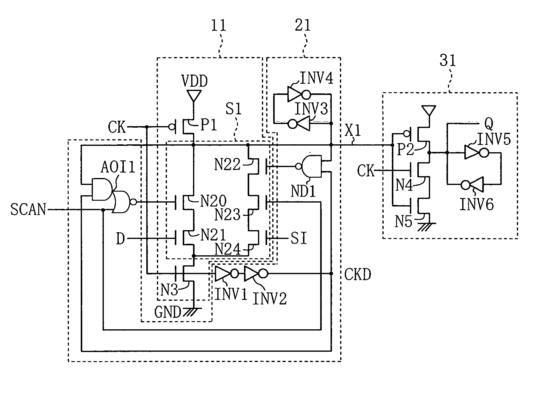
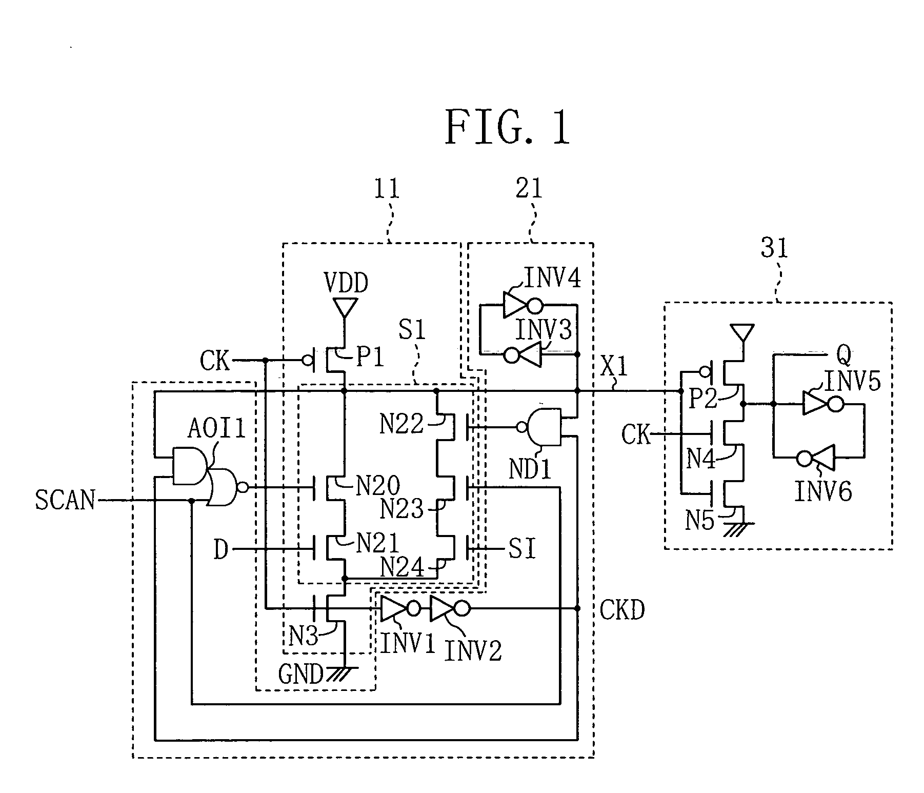
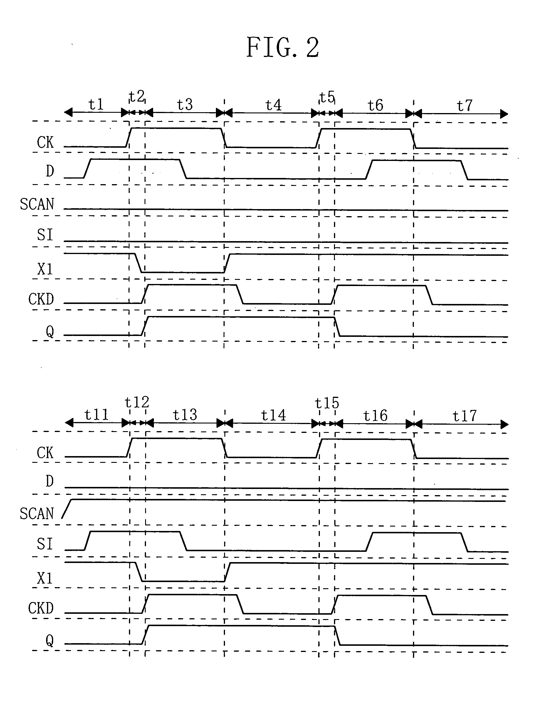
[0065]FIG. 1 is a circuit diagram showing a scan flip flop circuit according to embodiment 1 of the present invention. FIG. 2 is a timing chart which illustrates an operation of the scan flip flop circuit.

[0066] In FIG. 1, “D” denotes a data signal, “CK” denotes a clock signal, “SI” denotes a test input signal, “SCAN” denotes a test selection signal (including a data signal, a clock signal, a test input signal, first logic information of a test selection signal), “Q” denotes an output signal, “VDD” denotes a VDD power supply, and “GND” denotes a GND potential.

[0067] Reference numeral “AOI1” denotes an AND / OR inverter circuit which outputs an operation result of NOR logic of the output of a 2-input AND circuit and test selection signal SCAN. Reference numeral “ND1” denotes a 2-input NAND circuit. Reference numerals “N20” to “N24” denote nMOS transistors. A series connection of the nMOS trans...

Example

Embodiment 2

[0081] Hereinafter, a scan flip flop according to embodiment 2 of the present invention is described with reference to the drawings.

[0082]FIG. 3 is a circuit diagram showing a scan flip flop circuit according to embodiment 2. FIG. 4 is a timing chart which illustrates an operation of the scan flip flop circuit.

[0083] In the scan flip flop shown in FIG. 3, the input section 11 at the input side (including the pMOS transistor P1 and the nMOS transistors N20 to N24 and N3) and the output section 31 at the output side (including the pMOS transistor P2, the nMOS transistors N4 and N5, and the inverter circuits INV5 and INV6) have the same structures as shown in FIG. 1 in embodiment 1, and therefore, the descriptions thereof are omitted.

[0084] In embodiment 2, in the selector circuit S1 formed by the five nMOS transistors N20 to N24, a control section 22 for generating control signals which are input to the gate of the nMOS transistor N20 (third node X3 in FIG. 3) and the ...

Example

Embodiment 3

[0101]FIG. 5 is a circuit diagram showing a scan flip flop according to embodiment 3. FIG. 7 is a timing chart which illustrates an operation of the scan flip flop. It should be noted that, in embodiment 3, the same circuit components as those shown in the circuit diagrams of FIGS. 1 and 3 in embodiments 1 and 2 are denoted by the same reference numerals, and the descriptions thereof are omitted.

[0102] In embodiment 3, an input section 12, which includes the pMOS transistor P1, nMOS transistors N3, N20 to N24, is different from the input section 11 of embodiment 2 in that a selector circuit S1 formed by the nMOS transistors N20 to N24 is connected between the nMOS transistor N3 and the GND potential.

[0103] In the structure of FIG. 3 (embodiment 2), the nMOS transistor N6 and the pMOS transistor P4 are connected in series to the pMOS transistor P3 to constitute a transmission gate. However, in FIG. 5 of embodiment 3, only the nMOS transistor N6 is connected in series t...


PUM


Abstract

There is provided a flip flop circuit with a scan structure which is formed by an input section of a dynamic circuit and an output section of a static circuit wherein data is taken in within an interval of a short pulse width as compared with a clock cycle. In the dynamic circuit of the input section, the number of serially-connected MOS transistors to which a data signal is input is smaller than the number of serially-connected MOS transistors to which a test input signal is input. With this structure, the speed of operation is increased at the time of data storage for a data signal input, and the number of MOS transistors is reduced.

Description

CROSS-REFERENCE TO RELATED APPLICATIONS [0001] This application claims priority under 35 U.S.C. § 119(a) on Japanese Patent Application No. 2003-424603 filed on Dec. 22, 2003 and Japanese Patent Application No. 2004-336355 filed on Nov. 19, 2004, the entire contents of which are hereby incorporated by reference. BACKGROUND OF THE INVENTION [0002] The present invention relates to a scan flip flop which is capable of high speed operation and which can be formed by a small number of transistors. [0003] In a logic circuit of a semiconductor integrated circuit, a flip flop greatly influences the area, power consumption, and critical path delay, and therefore, reduction in the area of the flip flop, reduction in the power consumption, and higher processing speed have been demanded. A scan flip flop has been used in many devices for readily achieving a test for a designed LSI circuit. Especially, reduction in the area, reduction in the power consumption, and increase in the operation speed...

Claims


Application Information

Patent Timeline
IPC IPC(8): G01R31/3185H03K19/20
CPCG01R31/318541
Inventor HIRATA, AKIO
Owner PANASONIC CORP
Why Eureka
Try Eureka