Step edge insert ring for etch chamber

Inactive Publication Date: 2005-07-21
TAIWAN SEMICON MFG CO LTD
View PDF11 Cites 28 Cited by
  • Summary
  • Abstract
  • Description
  • Claims
  • Application Information

AI Technical Summary

Benefits of technology

[0021] In accordance with these and other objects and advantages, the present invention is generally directed to a new and improved insert ring for a wafer support inside a processing chamber for the processing, particularly dry etching, of semiconductor wafer substrates. The insert ring has a generally step-shaped cross-sectional configuration which defines a perpendicular gap or flow space between the insert ring and the outer wall or surface of the wafer support. Throughout etching of multiple successive substrates on the wafer support, the

Problems solved by technology

Decreased plasma intensity results in decreased, and thus incomplete, etching.
Increased plasma intensity, on the other hand, can cause overetching and plasma-induced damage of the wafers.
Plasma-induced damage includes trapped interf

Method used


Image

  • Step edge insert ring for etch chamber
  • Step edge insert ring for etch chamber
  • Step edge insert ring for etch chamber

Examples


Embodiment Construction

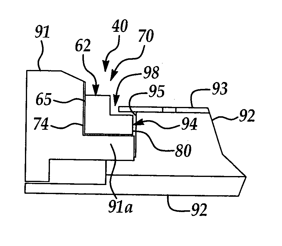
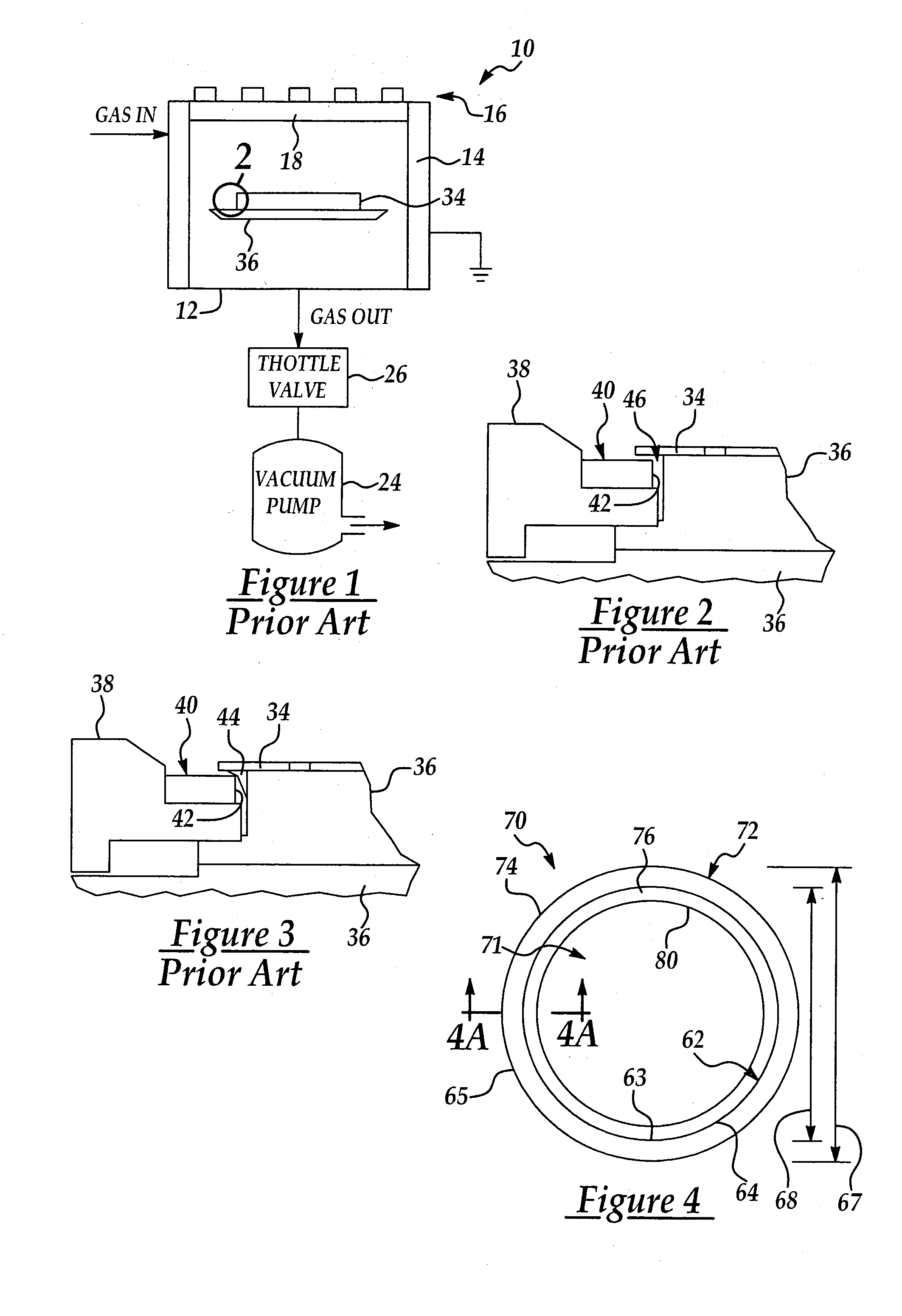
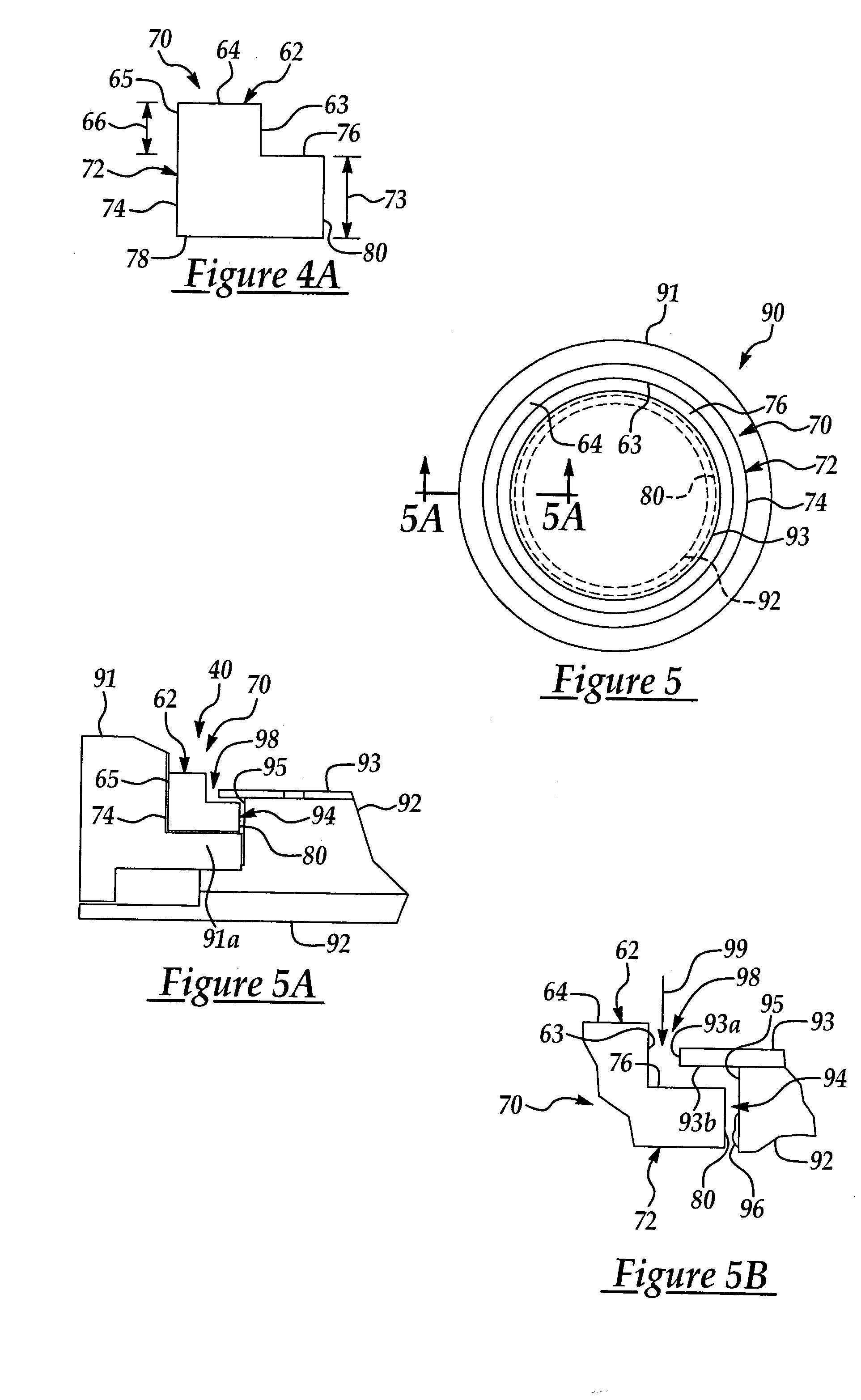
[0031] The present invention has particularly beneficial utility in preventing or reducing the rate of accumulation of polymer residues on the inner surface of an insert ring and / or a wafer support in an etching chamber for the etching of circuit patterns in semiconductor wafer substrates. However, the insert ring of the present invention may be equally applicable to preventing or minimizing the accumulation of polymer materials on the insert ring and / or wafer support during the use of various other types of process chambers used in the fabrication of integrated circuits, as well as process chambers or systems used in a variety of industrial applications.

[0032] Referring initially to FIGS. 4 and 4A, a preferred embodiment of the insert ring 70 of the present invention includes an annular ring body 72. A central ring opening 71 is defined by the ring body 72, as shown in FIG. 4. The ring body 72 is typically constructed of silicon and includes an outer ring surface 74, an upper ring...


PUM

PropertyMeasurementUnit
Thicknessaaaaaaaaaa
Thicknessaaaaaaaaaa
Flow rateaaaaaaaaaa

Abstract

An insert ring for a wafer support inside a processing chamber for the processing, particularly dry etching, of semiconductor wafer substrates. The insert ring has a generally step-shaped cross-sectional configuration which defines a perpendicular gap or flow space between the insert ring and the wafer support. In the etching of substrates on the wafer support, the perpendicular gap or flow space defines a perpendicular flow path for plasma species. Consequently, flow of heavy plasma species against the outer wall of the wafer support is substantially hindered or reduced to reduce accumulation of polymer material on the inner surface of the insert ring and/or the outer wall of the wafer support.

Description

FIELD OF THE INVENTION [0001] The present invention relates to etch chambers used to etch circuit patterns on semiconductor wafer substrates in the fabrication of integrated circuits on the substrates. More particularly, the present invention relates to a step edge insert ring that encircles an electrostatic chuck (ESC) in an etch chamber and provides a perpendicular gap space to substantially reduce polymer formation between the insert ring and the ESC, eliminating or reducing polymer peeling and B / H alarm activation between PM cycles. BACKGROUND OF THE INVENTION [0002] Integrated circuits are formed on a semiconductor substrate, which is typically composed of silicon. Such formation of integrated circuits involves sequentially forming or depositing multiple electrically conductive and insulative layers in or on the substrate. Etching processes may then be used to form geometric patterns in the layers or vias for electrical contact between the layers. Etching processes include “wet...

Claims


Application Information

Patent Timeline
IPC IPC(8): H01L21/00H01L21/687
CPCH01J37/32633Y10S156/915H01L21/68735H01L21/67069
Inventor HUANG, CHIH-WEICHANGCHIEN, SHIOW-FENGTANG, CHIA-HUNG
Owner TAIWAN SEMICON MFG CO LTD
Why Eureka
Try Eureka