Electrolytic processing apparatus and method

a processing apparatus and electrolysis technology, applied in the direction of electrolysis process, electrolysis components, tanks, etc., can solve the problems of not being able to meet the requirements of plating solutions, the development of plating solutions is facing such a difficult technical problem, and the production cost is reduced, so as to achieve the effect of reducing production costs and improving productivity

Inactive Publication Date: 2005-07-21
EBARA CORP
View PDF3 Cites 27 Cited by
  • Summary
  • Abstract
  • Description
  • Claims
  • Application Information

AI Technical Summary

Benefits of technology

[0020] The present invention has been made in view of the above situation in the related art. It is therefore an object of the present invention to provide an electrolytic processing apparatus and method which can produce products having various specifications with enhanced productivity, thus reducing the production cost, and which can respond flexibly to the movement toward finer interconnects in semiconductor devices.

Problems solved by technology

It is generally difficult with copper to form interconnects by anisotropic etching as practiced with aluminum.
The development of plating solutions is being confronted with such a difficult technical problem.
Ultrafine interconnects technology is a technology primarily for local interconnects, i.e. interconnects of the lower layers of a multi-layer interconnect structure, and probably may not be optimal, from a technical viewpoint and also in terms of cost, as a technology for forming global interconnects having an interconnect width of about 10 to 100 μm and a low aspect ratio.
It is therefore difficult to form interconnects of all the layers and efficiently produce a variety of devices with the use of a single plating solution as in the conventional electroplating apparatus.
Even when an apparatus construction that enables the use of two or more types of plating solutions, is adopted, if the operation is such that a specified electroplating unit is used solely for a particular plating solution, the apparatus can be operated only in an inflexible manner and at a high production cost.

Method used


Image

  • Electrolytic processing apparatus and method
  • Electrolytic processing apparatus and method
  • Electrolytic processing apparatus and method

Examples


Embodiment Construction

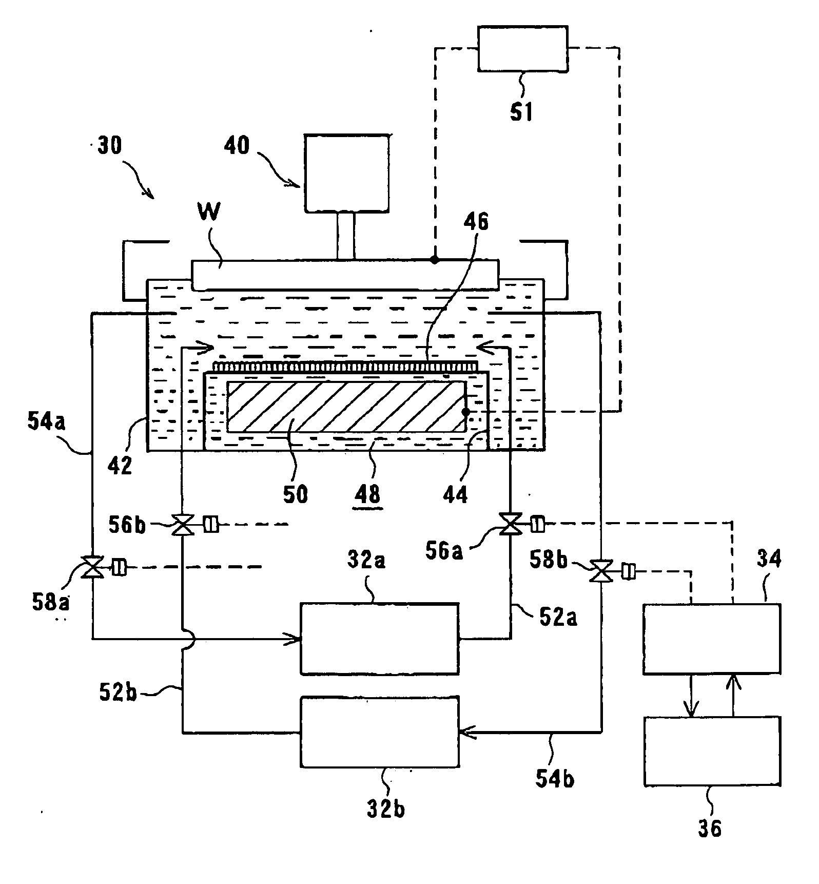
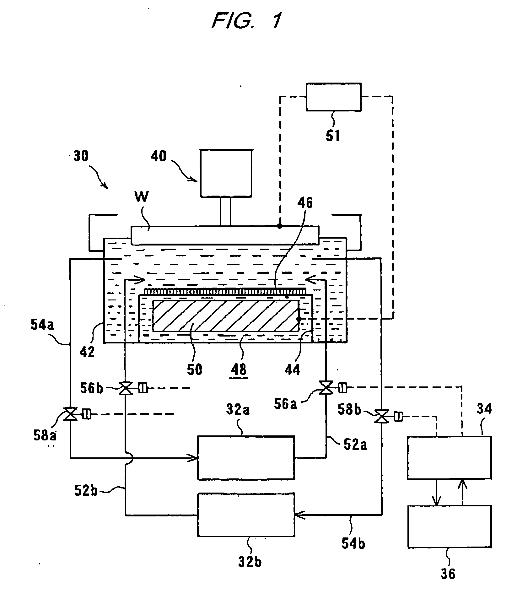
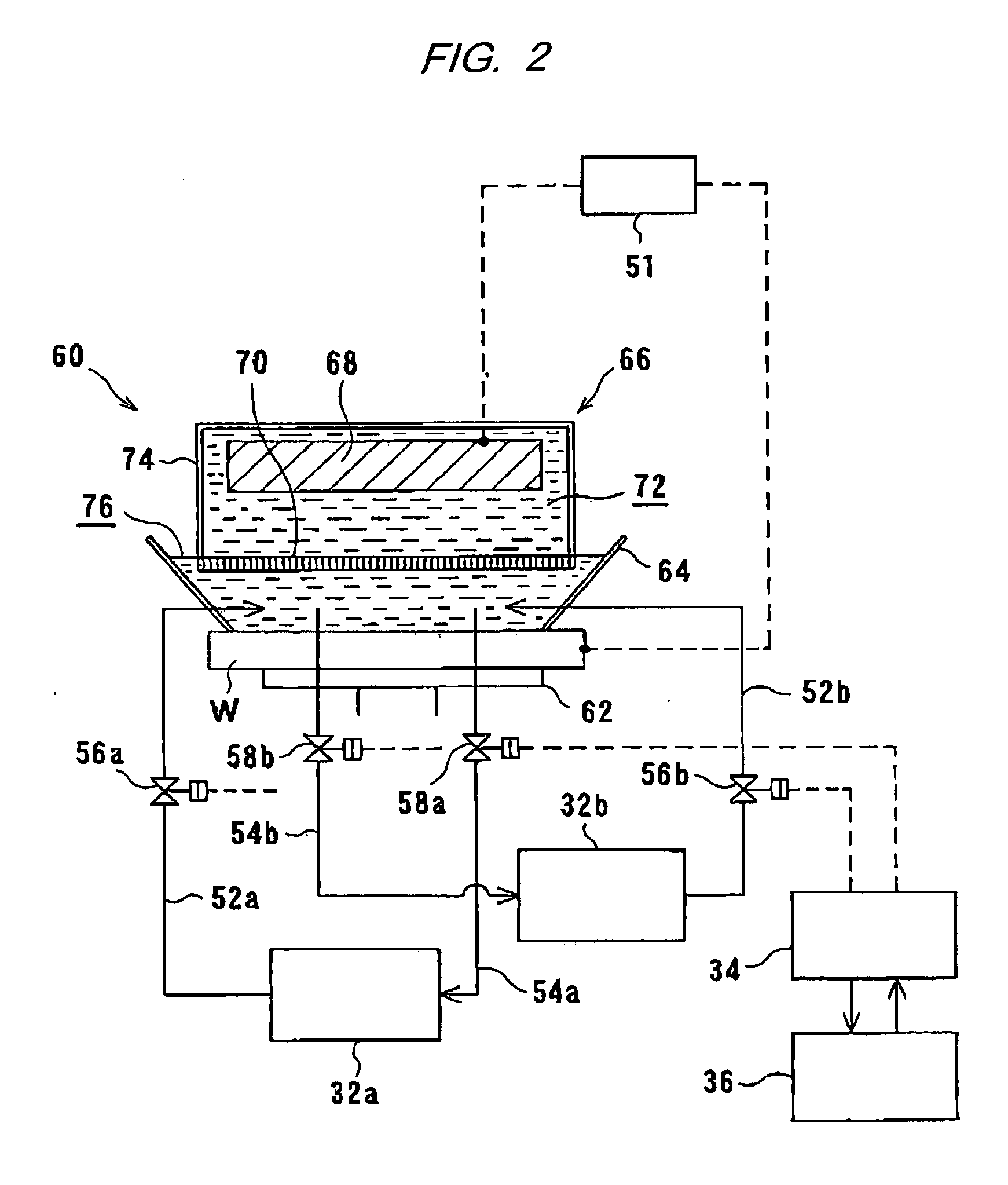
[0044] Preferred embodiments of the present invention will now be described with reference to the drawings. Though the following embodiments relate to application of the present invention to electroplating apparatuses, such apparatuses may of course be used as electrolytic etching apparatuses by applying a voltage, which allows an electric current to flow in a direction opposite to the direction of electric current in plating, between a substrate and a counter electrode plate while supplying an electrolysis solution (etching liquid) therebetween.

[0045]FIG. 1 is a schematic cross-sectional view of an electroplating apparatus (electrolytic processing apparatus) according to an embodiment of the present invention. As shown in FIG. 1, this electroplating apparatus includes an electroplating unit 30, two plating solution supply facilities (electrolysis solution supply facilities) 32a, 32b for supplying plating solutions as electrolysis solutions to the electroplating unit 30 and recover...


PUM

PropertyMeasurementUnit
widthsaaaaaaaaaa
widthaaaaaaaaaa
widthaaaaaaaaaa

Abstract

There is provided an electrolytic processing apparatus and method which can produce products having various specifications with enhanced productivity, thus reducing the production cost, and which can respond flexibly to the movement toward finer interconnects in semiconductor devices. An electrolytic processing apparatus according to the present invention includes: an electrolytic processing unit including a substrate holder for holding a substrate, and a counter electrode plate disposed opposite the substrate held by the substrate holder, said electrolytic processing unit carrying out electrolytic processing by filling the space between the substrate held by the substrate holder and the counter electrode plate with an electrolysis solution while feeding electricity; and a plurality of electrolysis solution supply facilities for supplying different types of electrolysis solutions; wherein the electrolytic processing unit is selectively connectable to one of the plurality of electrolysis solution supply facilities.

Description

BACKGROUND OF THE INVENTION [0001] 1. Field of the Invention: [0002] The present invention relates to an electrolytic processing apparatus and method, and more particularly to an electrolytic processing apparatus and method useful for forming, by plating, a film of an interconnect material, such as copper, on a substrate having fine interconnect patterns (recesses) formed in a surface, or for removing, by electrolytic etching, a metal film formed in a surface of a substrate. [0003] 2. Description of the Related Art: [0004] In recent years, instead of using aluminum or aluminum alloys as an interconnect material for forming electrical interconnects on a semiconductor substrate, there is an eminent movement toward using copper (Cu) which has a low electric resistivity and high electromigration endurance. It is generally difficult with copper to form interconnects by anisotropic etching as practiced with aluminum. Accordingly, copper interconnects are generally formed by the so-called ...

Claims


Application Information

Patent Timeline
Patent Type & Authority Applications(United States)
IPC IPC(8): C25B9/00C25D7/12C25D17/00C25D17/02C25D19/00C25D21/00
CPCC25D17/02C25D17/00
Inventor MISHIMA, KOJINAMIKI, KEISUKEHODAI, MASAOKUNISAWA, JUNJIMAKINO, NATSUKIFUKUNAGA, YUKIO
Owner EBARA CORP
Why Eureka
Try Eureka