Organic semiconductor structure, process for producing the same, and organic semiconductor device

a semiconductor device and organic semiconductor technology, applied in thermoelectric devices, sustainable manufacturing/processing, final product manufacturing, etc., can solve the problems of large grain boundary, large area, and inability to produce organic semiconductor layer as the element for constituting the organic semiconductor device substantially continuously in a satisfactory wide area with homogeneous properties and without difficulties. , to achieve the effect of excellent charge transfer characteristic and large area

Inactive Publication Date: 2005-07-21
DAI NIPPON PRINTING CO LTD
View PDF4 Cites 26 Cited by
  • Summary
  • Abstract
  • Description
  • Claims
  • Application Information

AI Technical Summary

Benefits of technology

[0014] According to the present invention, since the liquid crystalline organic semiconductor material is a liquid crystalline material which is fluid at such a temperature that can maintain the liquid crystal state, coating of the liquid crystalline organic semiconductor material onto a layer forming face or the formation of a layer of the liquid crystalline organic semiconductor material on a layer forming face, e.g., by vapor deposition followed by conversion of the state to a liquid crystal state is easy. The organic semiconducto

Problems solved by technology

Therefore, many grain boundaries are likely to exist, and, in addition, defects are likely to occur.
For this reason, in the formation of the organic semiconductor layer by film formation in vacuo, the organic semiconductor layer as the element for constituting the organic semiconductor device could not have been substantially continuously produced in a satisfactory wide area with homogeneous properties and without difficulties.
Therefore, close control of the molecular alignment is required, and this disadvantageously makes it difficult to utilize the discotic liqui

Method used


Image

  • Organic semiconductor structure, process for producing the same, and organic semiconductor device
  • Organic semiconductor structure, process for producing the same, and organic semiconductor device
  • Organic semiconductor structure, process for producing the same, and organic semiconductor device

Examples


examples

[0098] The following Examples further illustrate the present invention.

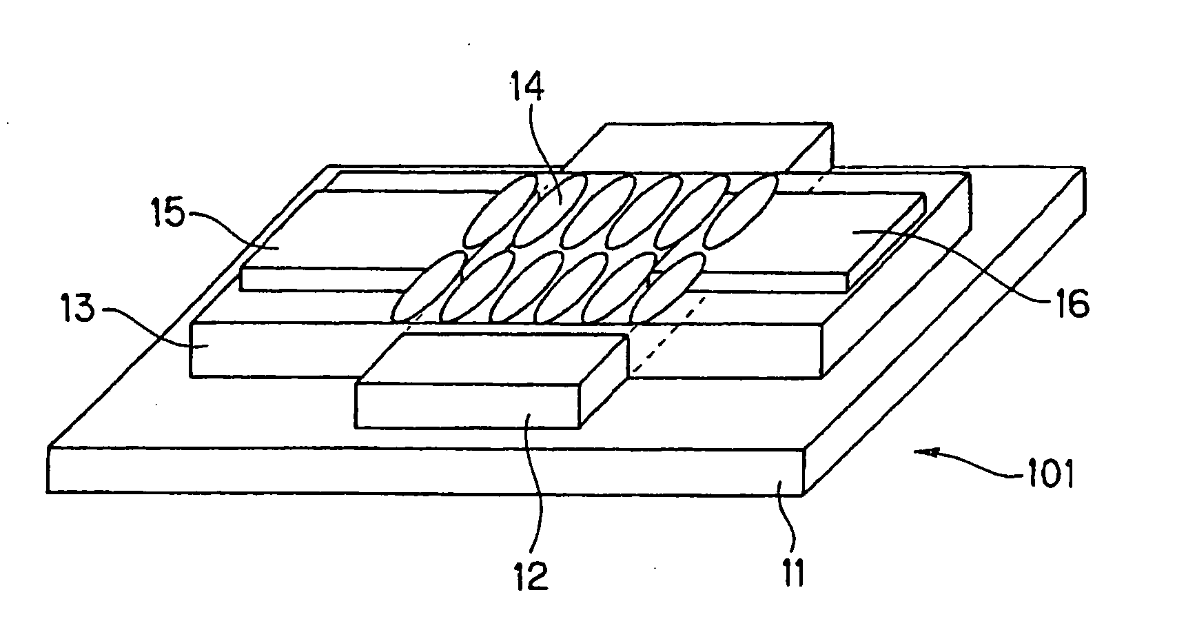
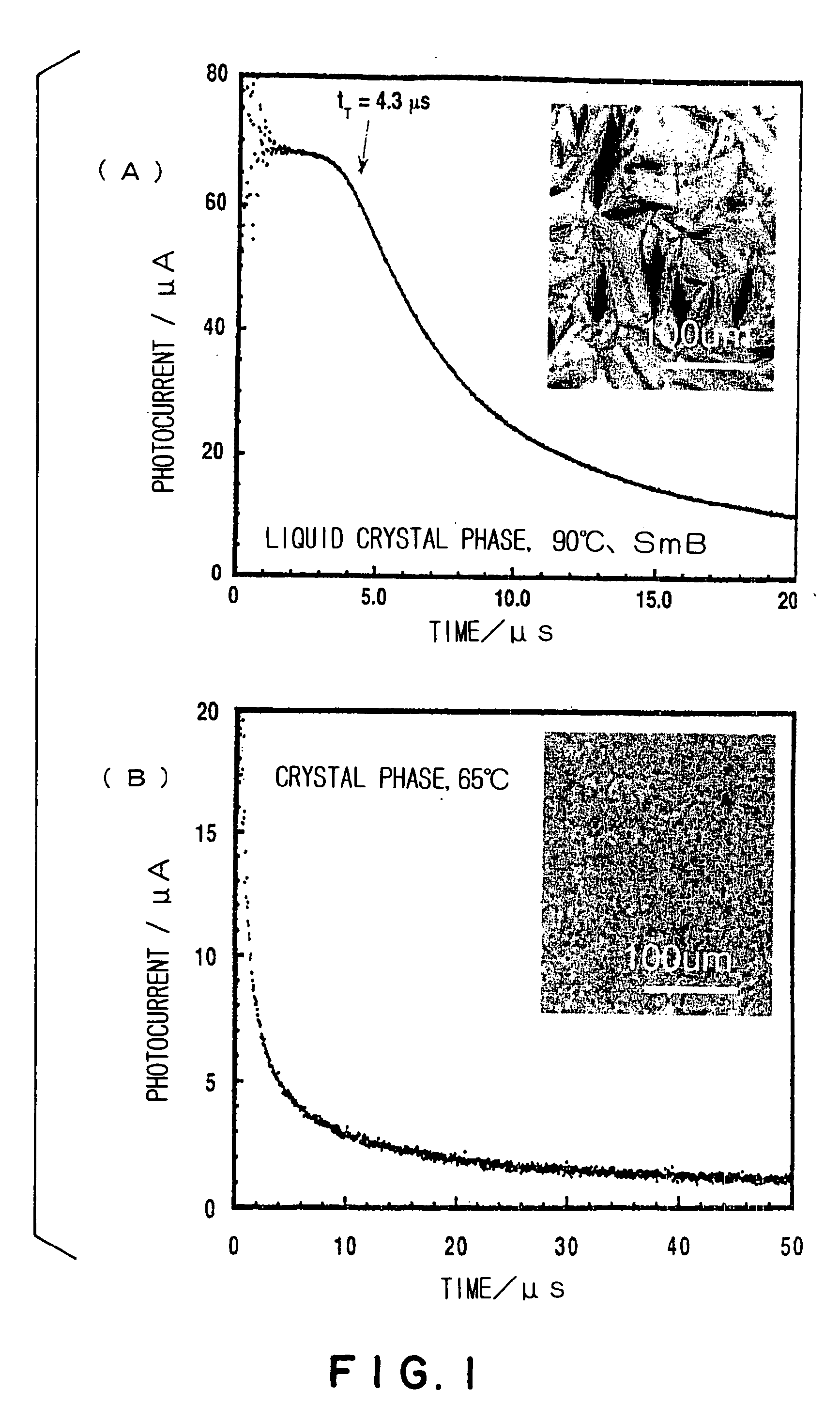
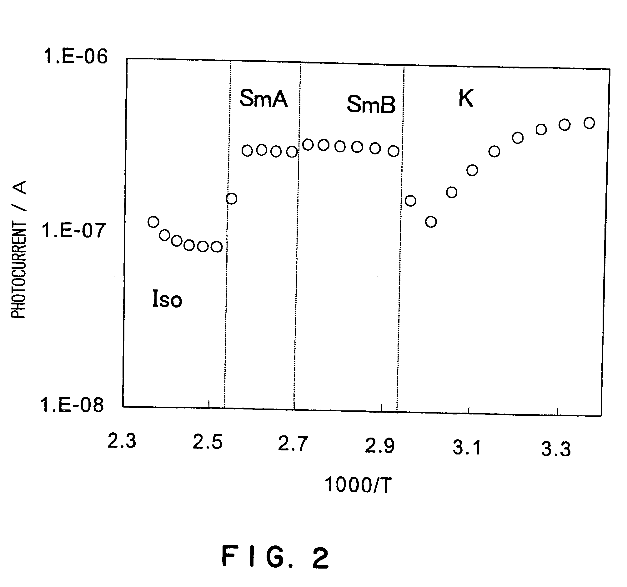
[0099] An organic semiconductor device having a construction of substrate / gate electrode / gate insulating layer (serving also as liquid crystal aligning layer) / source-drain electrode / liquid crystalline organic semiconductor layer ( / protective layer) was formed. In this Example, a layer of a liquid crystalline organic semiconductor material was formed on a glass substrate. The layer was then heated to a liquid crystal phase, thereby bringing the layer to a liquid crystal state. The layer was then gradually cooled to a crystal phase.

Substrate

[0100] A glass substrate (thickness 1.1 mm, Corning 1737), which had been ultrasonically cleaned with a neutral detergent, pure water, acetone, and IPA in that order, was used as a substrate.

Gate Electrode

[0101] A strip pattern (electrode width 100 μm, electrode spacing 5 mm) of gold (Au) (thickness 300 nm) was formed on the substrate through a metallic mask by resistance...


PUM


Abstract

There are provided an organic semiconductor structure comprising an organic semiconductor layer, which is large in size and homogeneous and has high charge transfer characteristics, a process for producing the same, and an organic semiconductor device. The organic semiconductor structure has, in at least a part thereof, an organic semiconductor layer comprising an aligned liquid crystalline organic semiconductor material. The liquid crystalline organic semiconductor material comprises an organic compound having a core comprising L 6 π electron rings, M 8 π electron rings, N 10 π electron rings, O 12 π electron rings, P 14 π electron rings, Q 16 π electron rings, R 18 π electron rings, S 20 π electron rings, T 22 π electron rings, U 24 π electron rings, and V 26 π electron rings, wherein L, M, N, O, P, Q, R, S, T, U, and V are each an integer of 0 (zero) to 6 and L+M+N+O+P+Q+R+S+T+U+V=1 to 6. The liquid crystalline organic semiconductor material exhibits at least one liquid crystal state at a temperature below the heat decomposition temperature thereof.

Description

TECHNICAL FIELD [0001] The present invention relates to an organic semiconductor structure comprising an organic semiconductor layer formed using a liquid crystalline organic semiconductor material, a process for producing the same, and an organic semiconductor device. BACKGROUND ART [0002] Thin-film transistors (also known as “organic TFT”) utilizing an organic semiconductor in an active layer (hereinafter referred to as “organic semiconductor layer”) may be mentioned as typical elements for constituting organic semiconductor devices. [0003] In the thin-film transistors, the organic semiconductor layer is formed by forming a film of a molecular crystal typified by pentacene in vacuo. Regarding the formation of the organic semiconductor layer by the film formation in vacuo, there is a report that the optimization of the film formation conditions can realize the formation of an organic semiconductor layer having a high level of charge mobility exceeding 1 cm2 / V·s (Y. -Y. Lin, D. J. G...

Claims


Application Information

Patent Timeline
IPC IPC(8): H01L29/786H01L35/24H01L51/00H01L51/30H01L51/40
CPCH01L51/0012Y02E10/549H01L51/0054H01L51/0055H01L51/0058H01L51/0062H01L51/0064H01L51/0067H01L51/0068H01L51/0069H01L51/0071H01L51/0076H01L51/0545H01L51/0558H01L51/057H01L51/0052Y02P70/50H10K71/191H10K85/623H10K85/649H10K85/652H10K85/656H10K85/622H10K85/615H10K85/655H10K85/626H10K85/654H10K85/731H10K85/657H10K10/491H10K10/484H10K10/466
Inventor HANNA, JUN-ICHIMAEDA, HIROKIAKADA, MASANORI
Owner DAI NIPPON PRINTING CO LTD
Why Eureka
Try Eureka