

High performance FET devices and methods thereof
a fet device, high-performance technology, applied in semiconductor devices, semiconductor/solid-state device details, electrical devices, etc., can solve the problems of short-channel effect, visible limits to straightforward downsizing, etc., to achieve high performance, low temperature operation, device performance
- Summary
- Abstract
- Description
- Claims
- Application Information
AI Technical Summary
Benefits of technology
Problems solved by technology
Method used
Image

Examples
Embodiment Construction
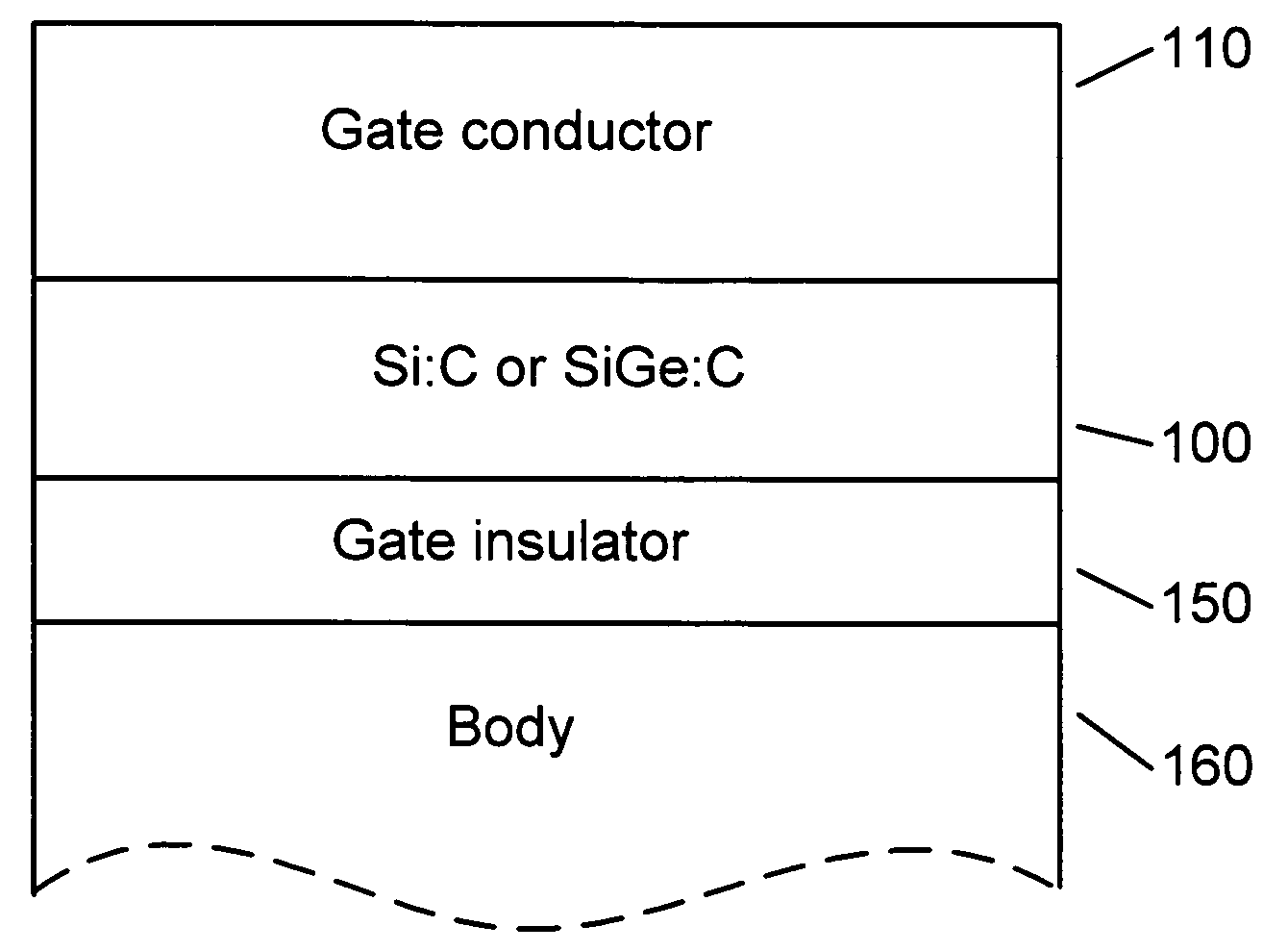
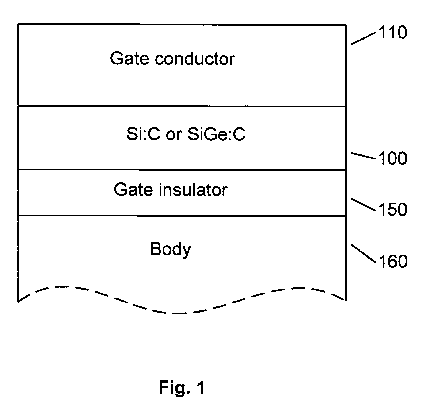
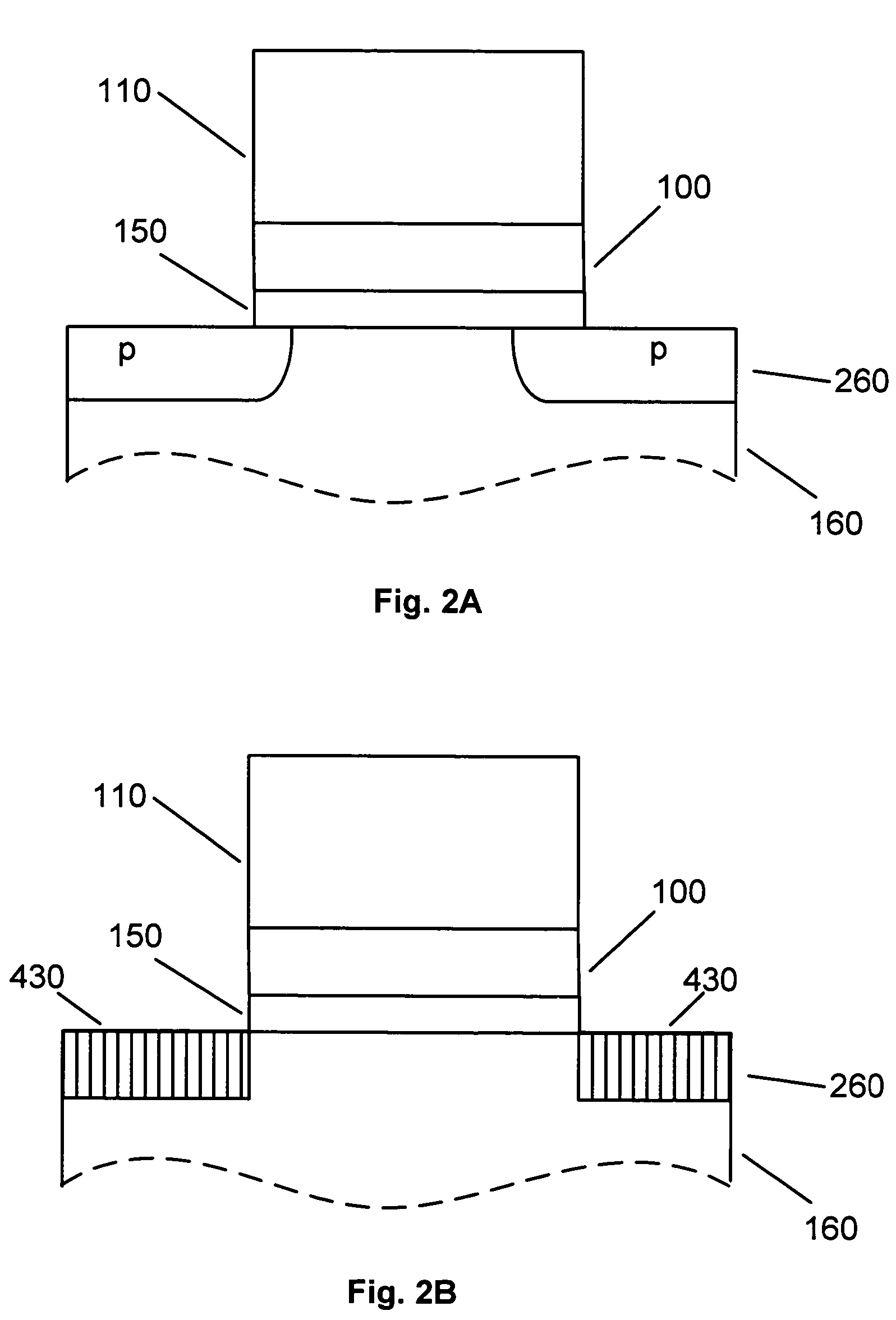
[0035] As the gate insulator, usually SiO2, thickness is being scaled down, i.e. below 5-10 nm, there is strong tendency that during any annealing, or rapid thermal annealing (RTA) steps, which are part of the device manufacturing process, the dopant originally in the polysilicon layer on the gate insulator diffuses through the gate insulator into the channel region of the MOSFET body. These dopants in the channel region would dramatically degrade the performance of the device. The doping level in the gate for 100 nm devices has to be at a very high level, i.e.>1021 / cm3. The common P-type dopant Boron (B) is the most prone to penetrate the gate insulator.
[0036] It was experimentally found that when a gate stack was made with two layers, a thin Si:C over the SiO2, followed by a heavily B doped polysilicon layer, then after annealing the gate using RTA at 1000° C. for 60 seconds, much of the boron from the P++ polysilicon layer was “arrested” within the poly-Si:C barrier layer, and v...
PUM
 Abstract
Description
Claims
Application Information