Beam light scanning device and image forming apparatus using same

a beam light scanner and beam light technology, applied in the direction of visual presentation using printers, instruments, electrographic processes, etc., can solve the problems of high purchasing price of light-emitting elements emitted beams of light in the marketplace, the apparatus as taught is faced, and the production cost of beam light scanner devices and image forming apparatuses using such scanners. achieve the effect of reducing production costs and reducing the number of light emission means

Inactive Publication Date: 2005-07-21
KK TOSHIBA +1
View PDF3 Cites 40 Cited by
  • Summary
  • Abstract
  • Description
  • Claims
  • Application Information

AI Technical Summary

Benefits of technology

[0005] It is therefore an object of this invention to avoid or mitigate the above-noted problem. It is another object of the invention to provide a technique for reducing p

Problems solved by technology

Unfortunately, the apparatus as taught thereby is faced with a problem which follows.
Commercially available LDs for use as the light-emitting elements that emit beams of light are high in purchasing price in the mar

Method used


Image

  • Beam light scanning device and image forming apparatus using same
  • Beam light scanning device and image forming apparatus using same
  • Beam light scanning device and image forming apparatus using same

Examples


first embodiment

[0017] the present invention will be described with reference to FIGS. 1 to 4 below.

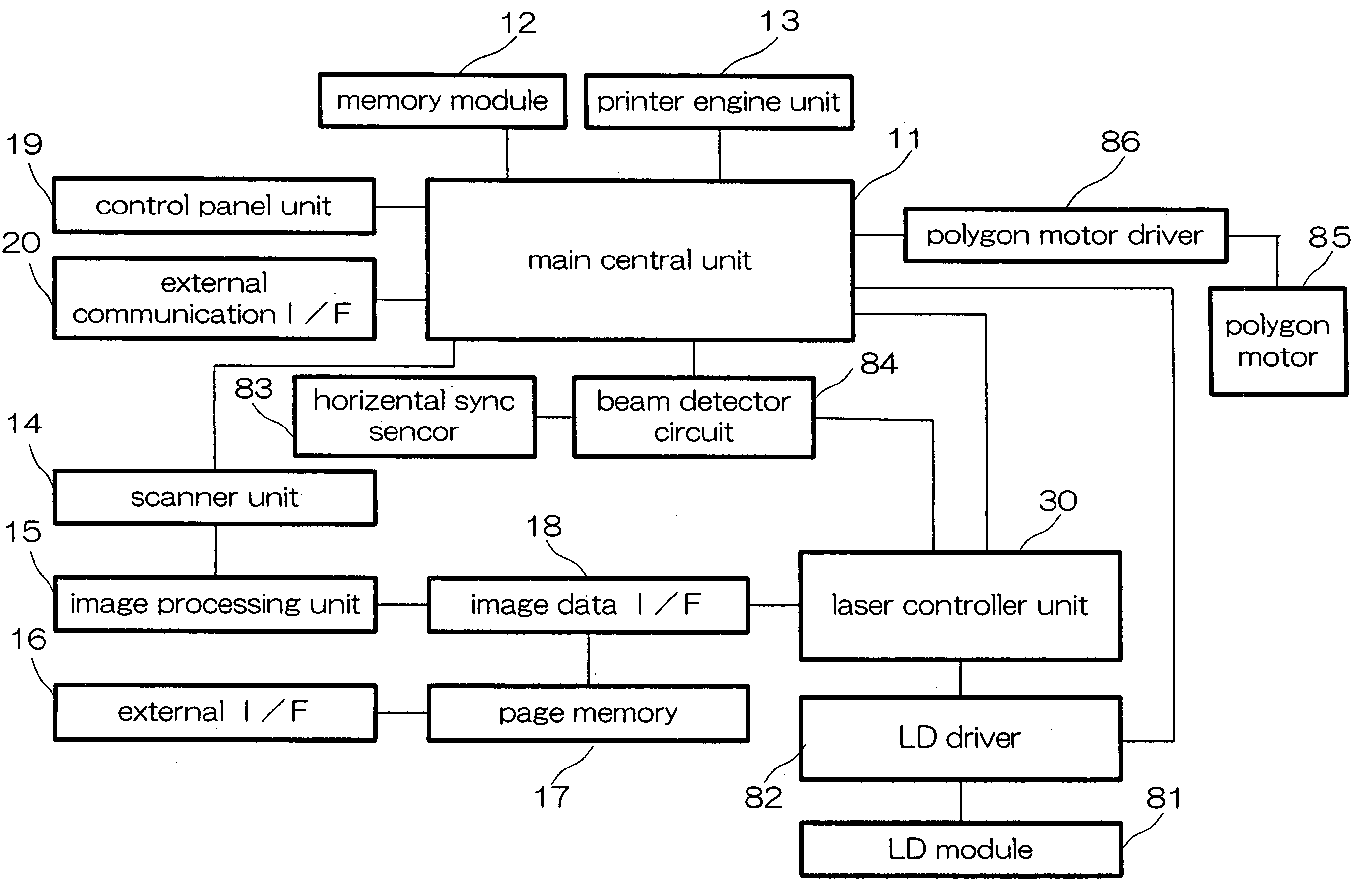
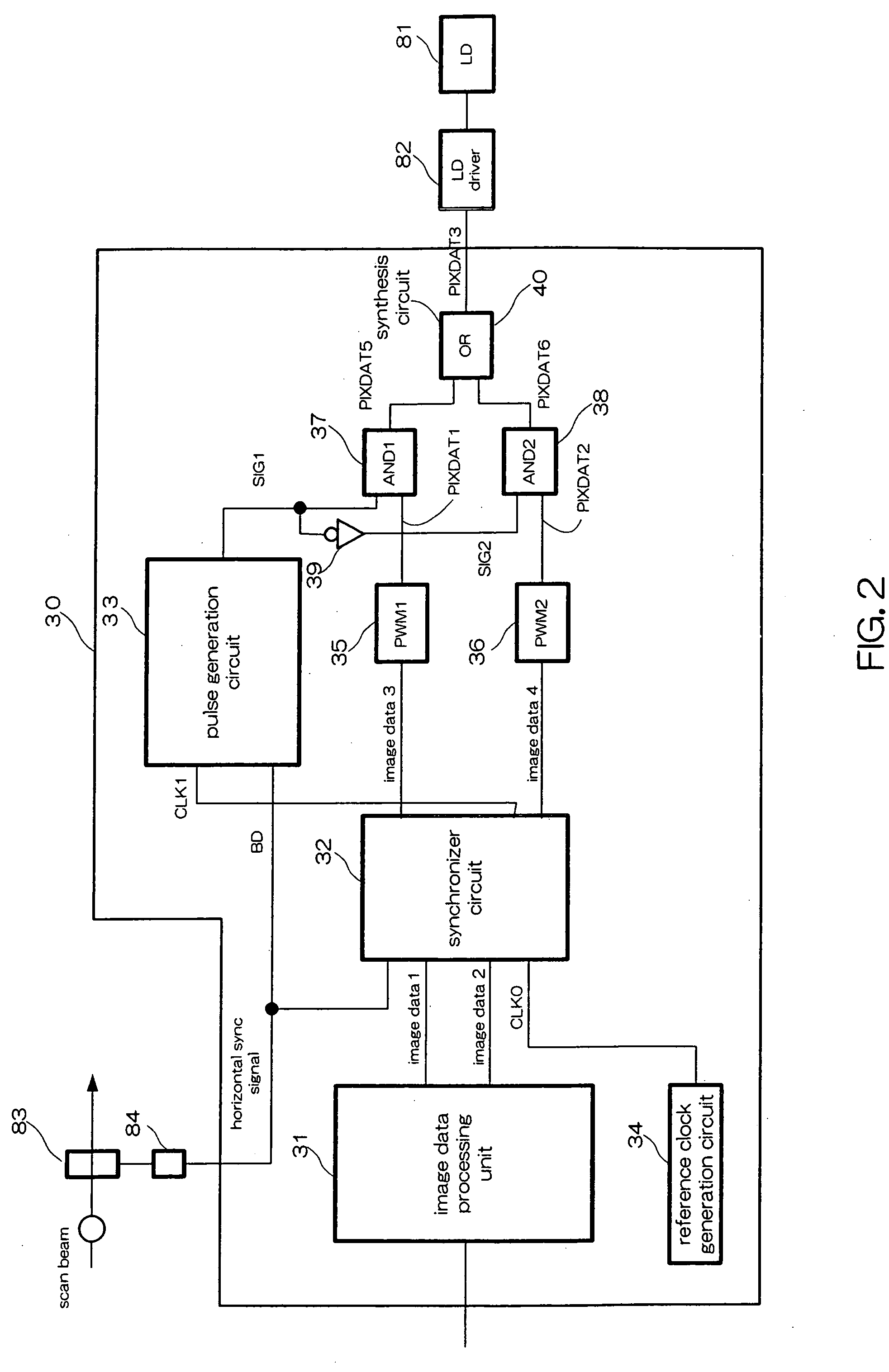
[0018]FIG. 1 is an electrical block diagram of an image forming apparatus, FIG. 2 is a detailed circuit diagram of electrical circuitry of part of a beam light scanning device, FIG. 3 is a diagram for explanation of pulse width adjustment and pulse positions of a pulse width modulator (PWM), and FIG. 4 is a timing chart of the first embodiment.

[0019] An explanation will first be given of an overall configuration of the image forming apparatus shown in FIG. 1. The image forming apparatus includes a main control unit 11 that provides control over an entirety of the image forming apparatus. This control unit 11 may be a central processor unit or “CPU.” This CPU 11 is operatively associated with a memory module 12 provided in the image forming apparatus. The memory module 12 is typically implemented as a read-only memory (ROM) that stores control tasks to be executed by the CPU 11 and a random access me...

second embodiment

[0056] Upon receipt of the second pixel data from the synchronizer circuit 52, the delay circuit 50 functions to cause outputting of the data to delay by a specified time within a time period equivalent to a single pixel output session. In the second embodiment, the delay circuit 50 delays it by a degree corresponding to one pixel, thereby providing a time-delayed output signal, which is then passed to the second PWM 56 via a line that indicates image data 4-2 in FIG. 5. Additionally a one-pixel delayed sync signal is input as a reference clock CLK2 to the pulse generator circuit 53.

[0057] There are input to the pulse generator circuit 53 the horizontal sync signal BD as output from the beam detector circuit 84 and the reference clock signal CLK1 that is synchronized by the synchronizer circuit 52 using the horizontal sync signal BD as output from beam detector 84. In addition, a reference clock signal CLK2 that was delayed by a specified time is also input from the delay circuit 50...

third embodiment

[0087] An operation of the third embodiment will next be discussed with reference to FIG. 8 below.

[0088] When a horizontal sync signal BD1 is output from the beam detector circuit 84 and then input to the synchronizer circuit 72a, the reference clock signal varies in cycle. In the third embodiment, upon rising up of the horizontal sync signal BD1, a reference clock signal CLK1 to be output from synchronizer 72a is changed to have a cycle which is shorter than the PWM period T1 stated previously. In addition, when a horizontal sync signal BD2 that was delayed by the delay circuit 70 is input to the second synchronizer circuit 72b, the reference clock signal changes in cycle. In the third embodiment, upon rising up of the sync signal BD2, the reference clock CLK1 to be output from second synchronizer 72b is modified to have a cycle which is shorter than the PWM period T1.

[0089] When the horizontal sync signal BD1 potentially falls down, the reference clock signal CLK1 being output fr...


PUM


Abstract

A beam light scanning device includes an image data processing unit operable to output image-processed data of neighboring pixels in such a way that the data is divided for distribution into first pixel data and second pixel data. The scanner also includes a synchronizer circuit that receives the first and second pixel data as output from the image data processor and outputs these pixel data while letting them be synchronized with clocks as synchronized based on a horizontal synchronous signal. The scanner further includes a couple of pulse width modulators or “PWMs”, a synthetic circuit, and a laser diode module. The PWMs are for adjustment of the pulse widths of the first and second pixel data as output from the synchronizer circuit respectively. The synthetic circuit combines together the pulse width-adjusted first and second pixel data. The LD emits a light beam indicative of the resultant combined pixel data.

Description

FIELD OF THE INVENTION [0001] The present invention relates to a beam light scanning device and image forming apparatus using the scanner device. BACKGROUND OF THE INVENTION [0002] Image forming apparatus of the type using electrophotography techniques is equipped with a beam light scanning device. The beam light scanner device has its light source, which is arranged by light-emitting elements such as laser diodes (LDs). In recent years, attempts are made to employ a plurality of LDs in order to speed up image formation operations. Output beams of individual LDs are guided to pass through a half mirror structure so that these are bundled together into substantially a single laser beam with prespecified beam intervals in a predetermined direction. The bundled laser beam is then guided to fall onto a polygon mirror. [0003] An example of this scheme is disclosed, for example, in Japanese Laid-Open Patent Application No. 2001-91873 (FIGS. 1 and 7). [0004] Unfortunately, the apparatus as...

Claims


Application Information

Patent Timeline
IPC IPC(8): B41J2/47G02B26/10G03G15/00G06K15/12H04N1/036H04N1/113H04N1/40H04N1/405
CPCG06K15/1223H04N1/1135H04N2201/0454H04N1/4056H04N1/40037
Inventor KOMIYA, KENICHITANIMOTO, KOJIISHIKAWA, DAISUKEINAGAWA, YUJI
Owner KK TOSHIBA
Why Eureka
Try Eureka