Electronic device and production method thereof

Inactive Publication Date: 2005-07-21
DAI NIPPON PRINTING CO LTD
View PDF10 Cites 31 Cited by
  • Summary
  • Abstract
  • Description
  • Claims
  • Application Information

AI Technical Summary

Benefits of technology

[0016] In the electronic device of the present invention, since the flange portion of the metal cap is fixed to the metal frame body of the uppermost-layer electronic component incorporating layer, falling off of the metal cap due to temperature cycle is prevented and further the heat radiation effect through the metal cap is achieved. Moreover, as compared with the conventional case where electronic components are externally mounted, size reduction of the electronic device is enabled. Further, as different from the conventional electronic device produced by stacking separate modules at a predetermined position by the use of connection means such as an anisotropic conductive film, a conductive adhesive, or a conductive paste, there is achieved an effect that fine-pitch connection is enabled, and further, high heat resistance and thus high reliability can be ensured.
[0017] Further, in the production method of the electronic device of the present invention, the insulating resin layer having a sufficient thickness for incorporating the e

Problems solved by technology

Consequently, size reduction of an electronic device is limited and tends to become further difficult as the number of electronic components to be mounted increases.
In the foregoing electronic device having the layered modules, however, connection means such as an anisotropic conductive film, a conductive adhesive, or a conductive paste is used for connection between each of the upper-lower side conducting vias forming the module and a corresponding one of wiring layers located under those vias, and there has been a problem that the width of selection of the connection means is narrowed i

Method used


Image

  • Electronic device and production method thereof
  • Electronic device and production method thereof
  • Electronic device and production method thereof

Examples


first embodiment

of Electronic Device

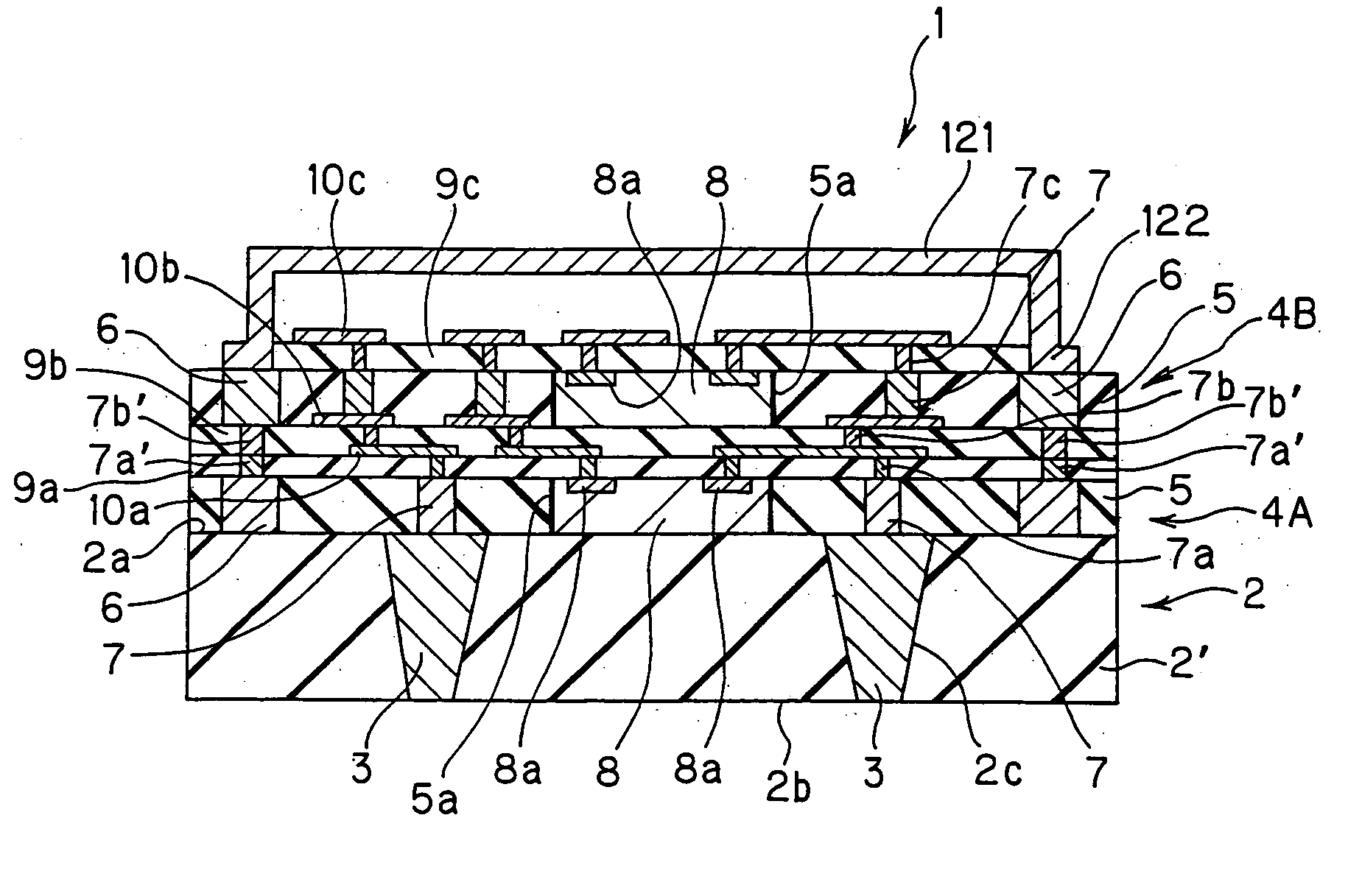
[0036]FIG. 1 is a schematic longitudinal sectional view showing one embodiment of an electronic device of the present invention. In FIG. 1, an electronic device 1 of the present invention comprises a core board 2, and wiring layers, electrically insulating layers, electronic component incorporating layers, and a metal cap which are formed on one surface 2a of the core board 2.

[0037] The core board 2 constituting the electronic device 1 comprises a core member 2′ and a plurality of through holes 2c formed in the core member 2′, and each through hole 2c is filled with a conductive material 3 so that electrical conduction between the front surface 2a and a back surface 2b of the core board 2 is established via each through hole 2c by the use of the conductive material 3. Each through hole 2c may have a straight shape having a substantially uniform inner diameter, a tapered shape in which an opening diameter at its one end is greater than that at its other end, a sh...

second embodiment

of Electronic Device

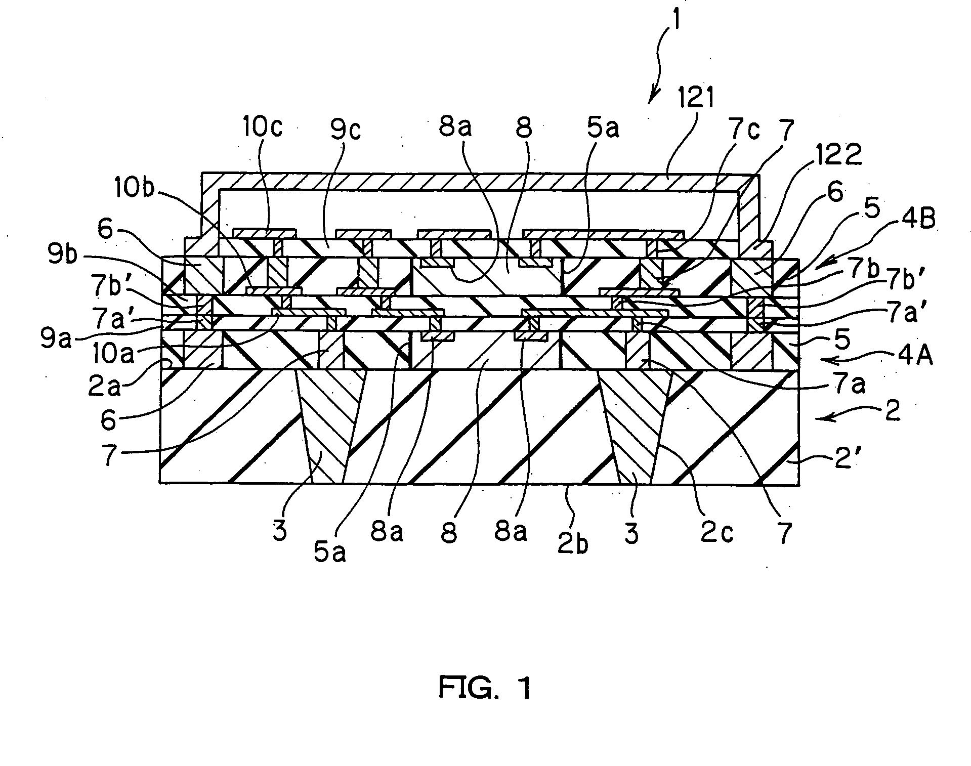
[0058]FIG. 2 is a schematic longitudinal sectional view showing another embodiment of an electronic device of the present invention. In FIG. 2, an electronic device 11 of the present invention comprises a core board 12, and wiring layers, electrically insulating layers, electronic component incorporating layers, and a metal cap which are formed on one surface 12a of the core board 12.

[0059] The core board 12 constituting the electronic device 11 comprises a core member 12′ and a plurality of through holes 12c formed in the core member 12′, and each through hole 12c is filled with a conductive material 13 so that electrical conduction between the front surface 12a and a back surface 12b of the core board 12 is established via each through hole 12c by the use of the conductive material 13. In the illustrated example, each through hole 12c has a tapered shape.

[0060] An electronic component incorporating layer 14A is formed on the surface 12a of the core board 12 c...

third embodiment

of Electronic Device

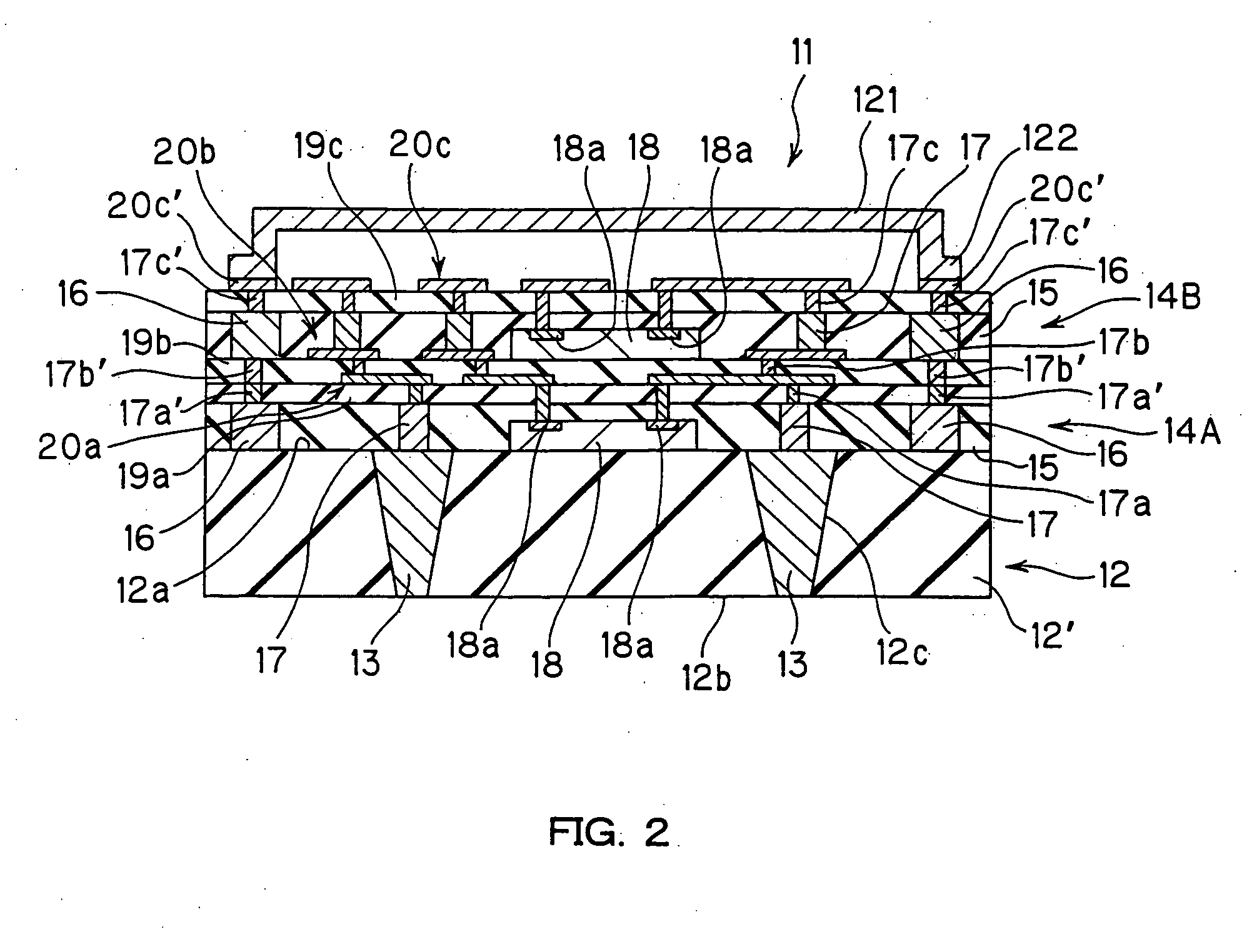
[0075]FIG. 3 is a schematic longitudinal sectional view showing another embodiment of an electronic device of the present invention. In FIG. 3, an electronic device 21 of the present invention comprises a stacked or layered body having wiring layers, electrically insulating layers, and electronic component incorporating layers, external terminal wiring layers, and a metal cap.

[0076] In the electronic device 21, an electronic component incorporating layer 24A is formed on external terminal wiring layers 23. The electronic component incorporating layer 24A comprises an insulating resin layer 25, an electronic component 28 received in a cutout portion 25a formed in the insulating resin layer 25, and upper-lower side conducting vias 27 and further comprises a metal frame body 26 disposed near a peripheral portion of the insulating resin layer 25 so as to surround the upper-lower side conducting vias 27 and the electronic component 28. The upper-lower side conducting...


PUM


Abstract

An object is to provide an electronic device of a multilayer structure with high density and high reliability that can be reduced in size while incorporating an electronic component therein, and further provide a production method for easily producing such an electronic device. An electronic device of the present invention includes wiring layers and electrically insulating layers stacked on a core board and establishes predetermined electrical conduction between the wiring layers through upper-lower side conducting vias provided in the electrically insulating layers. An electronic component incorporating layer formed by directly forming on a lower layer an insulating resin layer having a cutout portion for receiving an electronic component therein and upper-lower side conducting vias and by incorporating the electronic component in the cutout portion is provided at least between one of the wiring layers and one of the electrically insulating layers and/or between the core board and the electrically insulating layer. At least the uppermost-layer electronic component incorporating layer of electronic component incorporating layers has a metal frame body surrounding the electronic component and the upper-lower side conducting vias, and a metal cap having a flange portion fixed to the metal frame body of the uppermost-layer electronic component incorporating layer is provided.

Description

BACKGROUND OF THE INVENTION [0001] The present invention relates to an electronic device, particularly an electronic device having an electronic component such as an LSI chip incorporated therein, and further relates to a production method of such an electronic device. [0002] A conventional multilayer wiring board is produced by, for example, using as a core board a double-sided board having low density wiring formed by the subtractive method or the like, and forming high density wiring on each side of the core board by the buildup method. On the other hand, the bare chip mounting method has been recently proposed wherein an LSI chip or the like is directly mounted onto a multilayer wiring board. In the bare chip mounting method, a semiconductor chip is mounted onto a connection pad portion of wiring formed on a multilayer wiring board in advance, by the use of connection means such as a bonding wire, bumps formed by solder, metal balls or the like, an anisotropic conductive film, a...

Claims


Application Information

Patent Timeline
IPC IPC(8): H01L21/68H01L25/18H01L23/02H01L23/538H01L25/065H01L25/07H05K1/18H05K3/46
CPCH01L21/6835H01L23/5389H01L2924/07802H01L24/18H01L24/82H01L25/0657H01L2221/68345H01L2224/18H01L2224/82001H01L2225/06524H01L2225/06527H01L2225/06541H01L2225/06582H01L2924/01013H01L2924/01027H01L2924/01029H01L2924/01078H01L2924/01079H01L2924/04941H01L2924/09701H01L2924/14H01L2924/18162H01L2924/19041H01L2924/19042H05K1/185H05K3/4602H01L2924/01005H01L2924/01006H01L2924/01019H01L2924/01024H01L2924/01033H01L2924/01047H01L2924/014H01L2224/73267H01L2924/00H01L2924/12042H01L24/19H01L24/20H01L2224/04105H01L2224/12105H01L2224/32225H01L2224/92244H01L2224/19H01L2224/83005
Inventor KURAMOCHI, SATORUFUKUOKA, YOSHITAKA
Owner DAI NIPPON PRINTING CO LTD
Why Eureka
Try Eureka