

Method for forming interconnection line in semiconductor device and interconnection line structure
a technology of interconnection lines and semiconductor devices, which is applied in the direction of basic electric elements, transportation and packaging, transportation items, etc., can solve the problems of resisting-capacitance delay, slowing electrical signals throughout the circuit, and slowing the total operational speed of the semiconductor devi
- Summary
- Abstract
- Description
- Claims
- Application Information
AI Technical Summary
Benefits of technology
Problems solved by technology
Method used
Image

Examples
first embodiment
[0019]FIG. 1 to FIG. 4 are cross-sectional views illustrating a method for forming an interconnection line of a semiconductor device in accordance with the present invention.
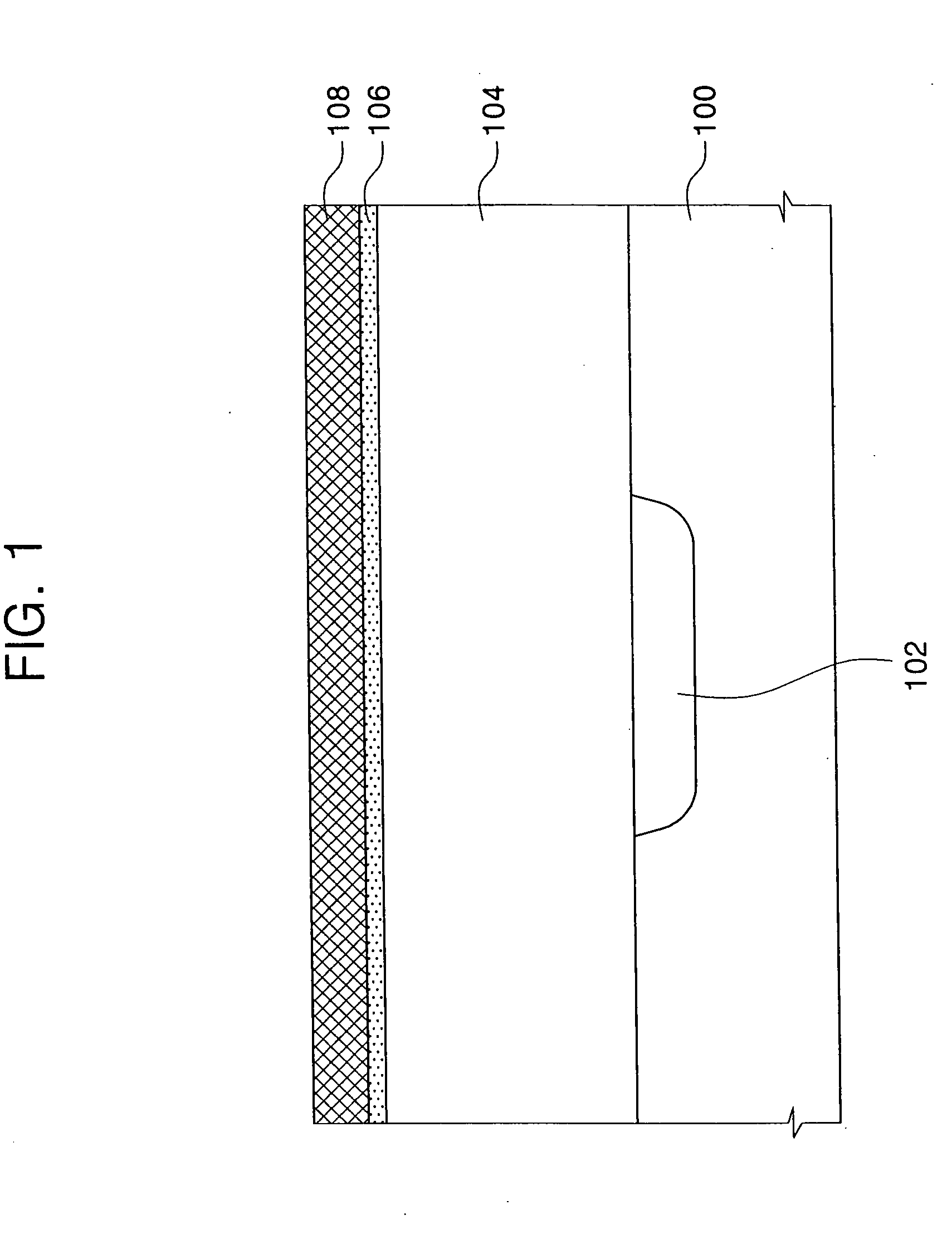
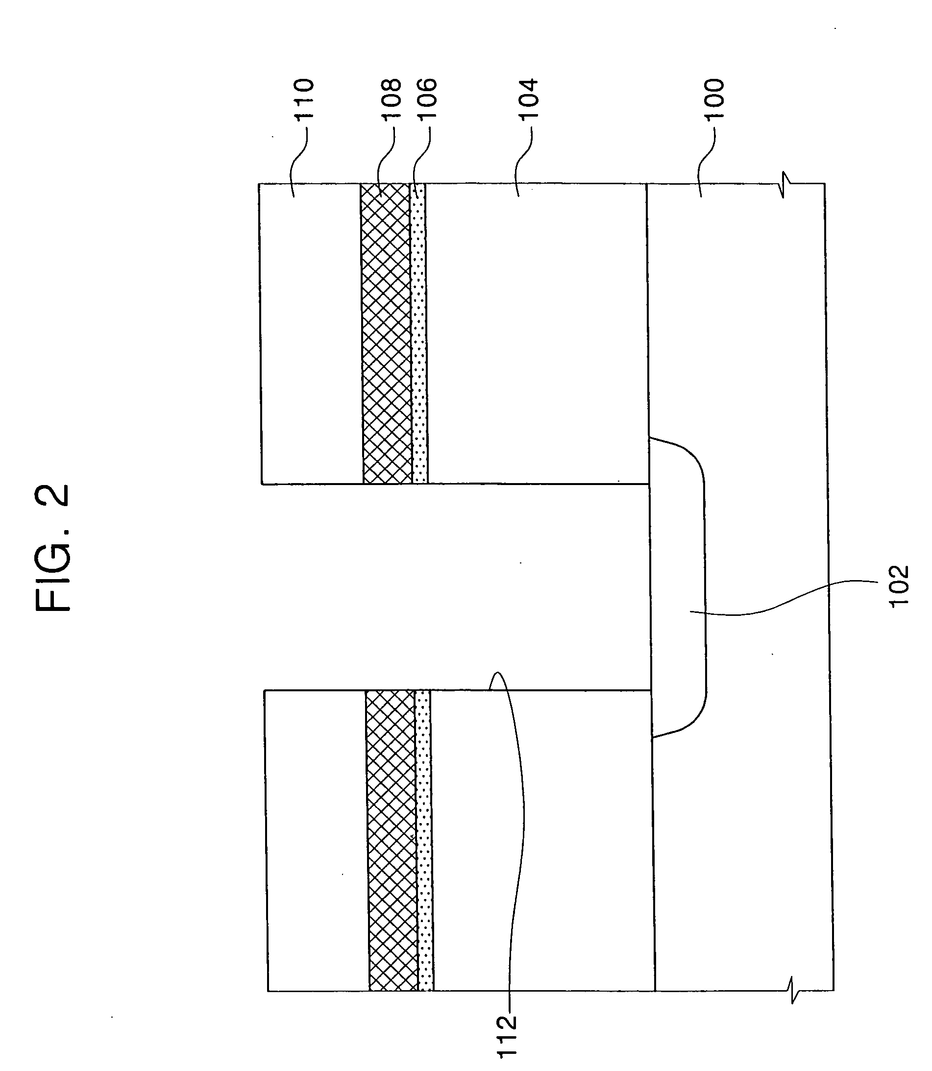
[0020] Referring to FIG. 1, an interlayer insulating layer 104 is formed on a semiconductor substrate 100. A conductive region 102 is formed in semiconductor substrate 100. Conductive region 102 is preferably an impurity diffusion region having P type or N type impurity ions implanted therein. Interlayer insulating layer 104 is formed of a low-k carbon-doped dielectric material. In the embodiments of the present invention, the low-k dielectric material has a dielectric constant lower than silicon oxide, which has a dielectric constant of about 4. Interlayer insulating layer 104 is preferably formed of an OSG layer of SiOC or SiOCH. For example, the low-k carbon-doped dielectric layer is an organic spin-on polymer layer such as SiLK™, which is available from Dow Chemical Co. When interlayer insulating layer 104 i...
second embodiment
[0029]FIG. 5 to FIG. 11 are cross-sectional views illustrating a method for forming an interconnection line of a semiconductor device in accordance with the present invention.
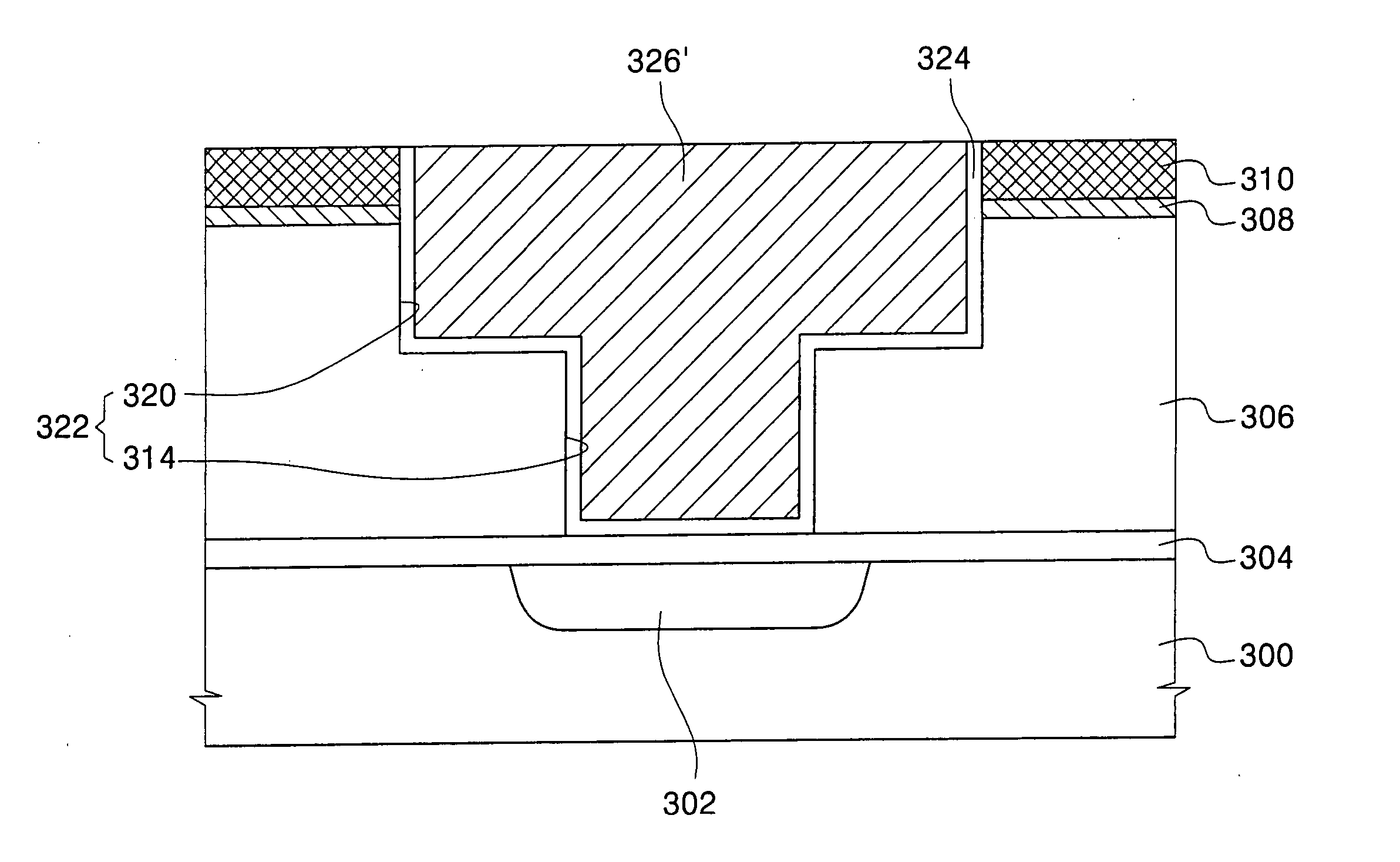
[0030] Referring to FIG. 5, an etch-stop layer 304 is formed on a semiconductor substrate 300. A conductive region 302 is formed in semiconductor substrate 300. Conductive region 302 is preferably an impurity diffusion region formed by implanting P type or N type impurity ions into semiconductor substrate 300. Etch-stop layer 304 is preferably formed of SiN, SIC, or SiCN. Etch-stop layer 304 prevents conductive region 302 from being exposed and damaged in a subsequent wet cleaning process or a subsequent anisotropic etching process to form a via hole. The same methods and materials may be applied as in the first embodiment to successively form an interlayer insulating layer 306 of low-k carbon-doped dielectric material, oxidation barrier layer 308, and oxide capping layer 310. Oxidation barrier layer 308 is pre...
third embodiment
[0043]FIG. 12 and FIG. 13 are cross-sectional views illustrating a method for forming an interconnection line of a semiconductor device in accordance with the present invention.
[0044] Referring to FIG. 12, a lower etch-stop layer 504, a first interlayer insulating layer 506, an upper etch-stop layer 508, and a second interlayer insulating layer 510 are successively formed on a semiconductor substrate 500 having a conductive region 502. Each of lower etch-stop layer 504 and upper etch-stop layer 508 is preferably SiN, SiC, or SiCN. First interlayer insulating layer 506 is preferably formed of low-k carbon-doped dielectric material as discussed in the first and second embodiments, but may be formed of a material that has a dielectric constant higher than that of the low-k carbon-doped dielectric material. In other words, first interlayer insulating layer 506 may be formed of a silicon oxide layer, a phosphor silicate glass (PSG) layer, a USG layer, an FSG layer, high density plasma (H...
PUM
 Abstract
Description
Claims
Application Information