

Integrated circuit device
- Summary
- Abstract
- Description
- Claims
- Application Information
AI Technical Summary
Benefits of technology
Problems solved by technology
Method used
Image

Examples
Embodiment Construction
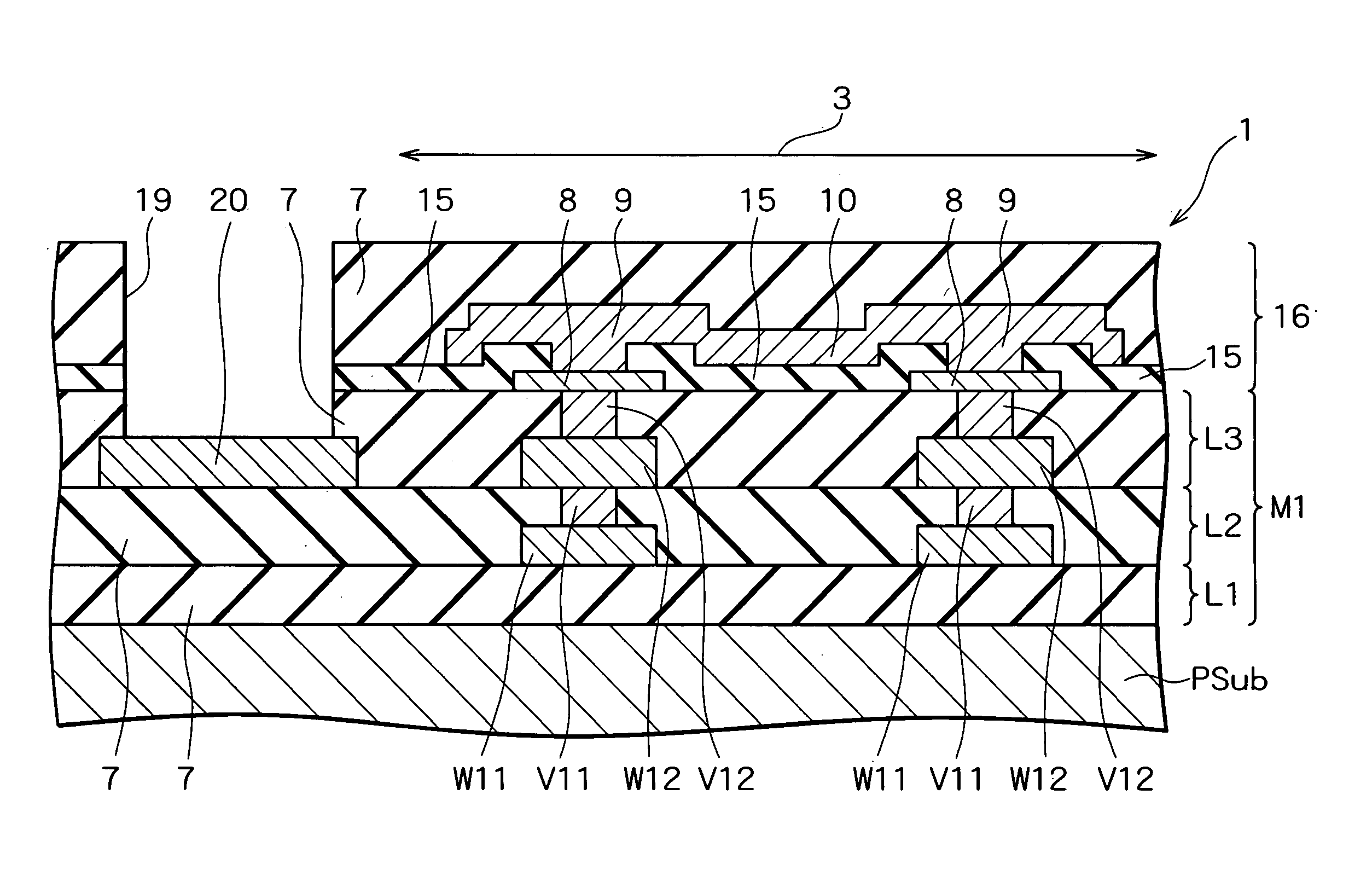
[0033] Preferred embodiments of the present invention will be described specifically below with reference to the accompanying drawings. To begin with, a first embodiment of the present invention will be discussed. FIG. 3 is a cross-sectional view showing a semiconductor integrated circuit device according to the first embodiment of the invention, and FIG. 4 is an equivalent circuit diagram showing the temperature sensor section of the semiconductor integrated circuit device shown in FIG. 3. The semiconductor integrated circuit device according to the present embodiment is formed on a single silicon chip. As shown in FIG. 3, the semiconductor integrated circuit device 1 according to the embodiment is provided with a temperature sensor section 3, a logic circuit section (not shown) and an external pad to connect the internal circuit of the semiconductor integrated circuit device 1 to an external device. The following will describe the structure that is common to the entire semiconduct...
PUM
 Abstract
Description
Claims
Application Information