Current limiter of output transistor

Inactive Publication Date: 2005-07-28
RENESAS ELECTRONICS CORP
View PDF3 Cites 6 Cited by
  • Summary
  • Abstract
  • Description
  • Claims
  • Application Information

AI Technical Summary

Benefits of technology

[0022] The present invention places a current mirror circuit between a current detection circuit and a protection transistor, thereby achieving a maximum output current while preventing thermal destruction of an output MOS transistor.

Problems solved by technology

Thus, overcurrent causes thermal destruction of the output MOS transistor.
If the drain-source voltage of the power output MOS transistor increases, the energy in the output MOS transistor increases accordingly, which can ultimately cause the self-destruction of the output MOS transistor.
However, merely reducing the output current results in decrease in the obtained output current, impeding the power output MOS transistor from functioning satisfactory.
Thus, a high limiting current causes destruction of the output MOS transistor 64.
This technique, however, requires a large size of circuit and fails to obtain a smooth waveform of the limiting current.

Method used


Image

  • Current limiter of output transistor
  • Current limiter of output transistor
  • Current limiter of output transistor

Examples


Embodiment Construction

[0033] The invention will be now described herein with reference to illustrative embodiments. Those skilled in the art will recognize that many alternative embodiments can be accomplished using the teachings of the present invention and that the invention is not limited to the embodiments illustrated for explanatory purposed.

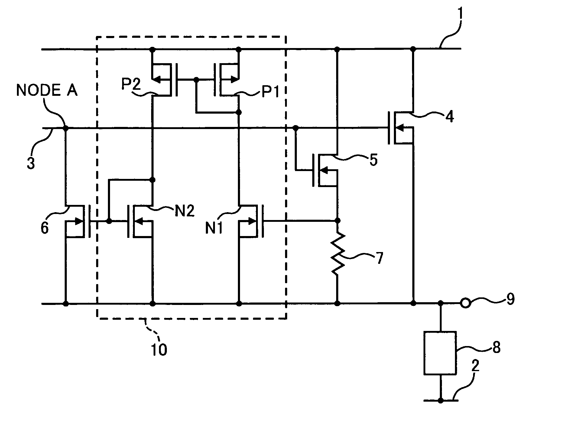
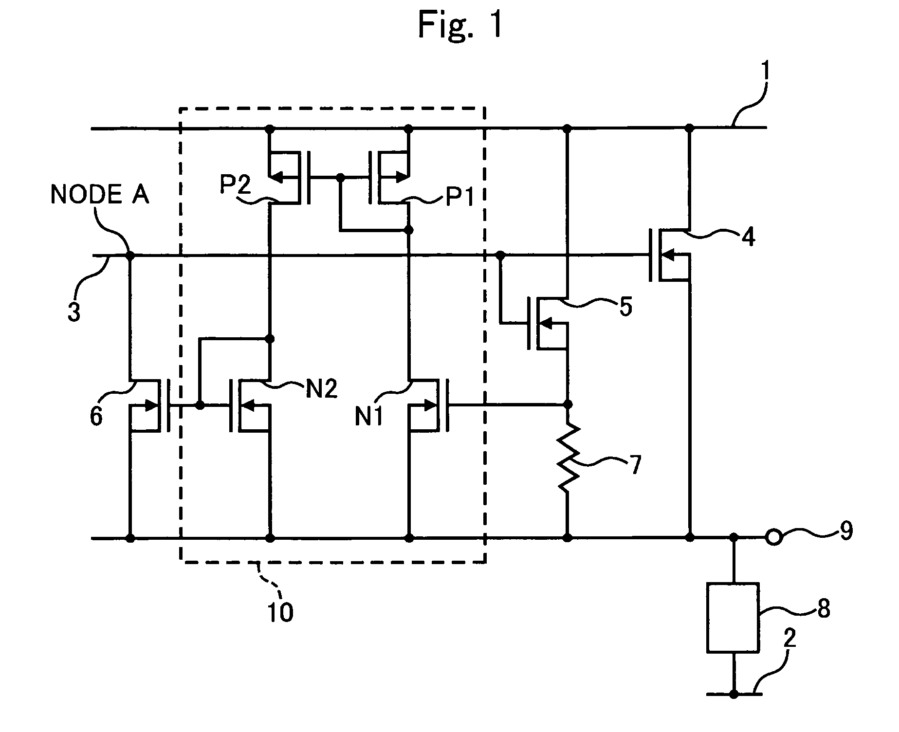
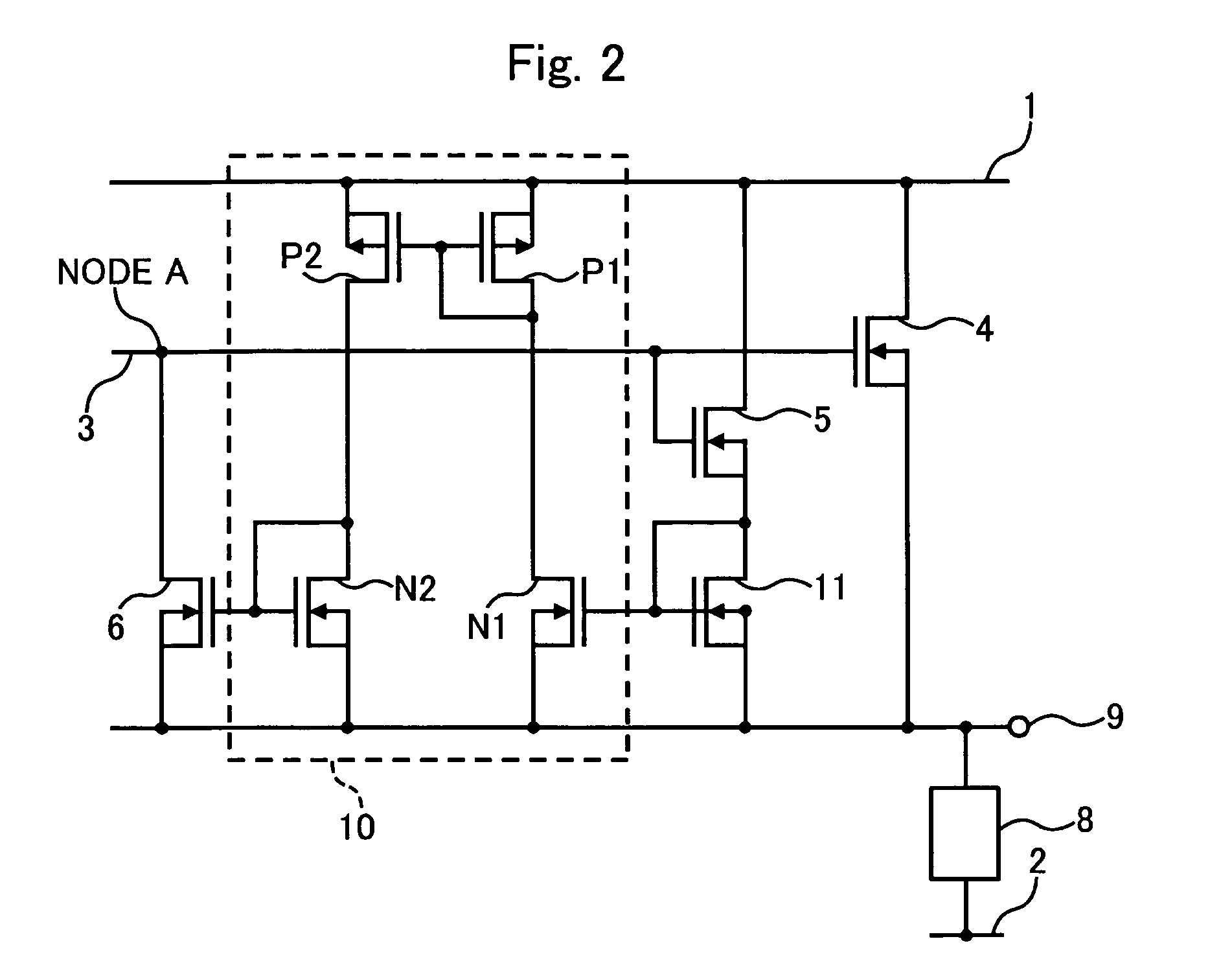
[0034] An embodiment of the invention is explained hereinafter in detail with reference to the drawings. Referring first to FIGS. 1 and 2, the current limiters include an Nch source follower in which an output MOS transistor 4 and a load 8 are connected in series between a first power supply 1 and a second power supply 2. An output terminal 9 is connected to a connection node of the output MOS transistor 4 and the load 8. The output MOS transistor 4 is turned on or off according to a first control signal 3 inputted to the gate terminal. The current limiters also have a current detection MOS transistor 5. A given ratio exists between the current detection MOS tr...


PUM


Abstract

A current limiter of an output transistor comprises an output transistor, a current detection transistor monitoring a current flowing through the output transistor, a current mirror circuit, a protection transistor outputting a current having passed through the current mirror circuit, the current being proportional to the monitored current and dependent on a voltage between a drain and a source or between a collector and an emitter of the output transistor and an input terminal connected to an output of the protection transistor.

Description

BACKGROUND OF THE INVENTION [0001] 1. Field of the Invention [0002] The present invention relates to power semiconductor devices and particularly to a device having a current limiter of an output transistor. [0003] 2. Description of the Related Art [0004] A power semiconductor device includes an input circuit, an output metal oxide semiconductor (MOS) transistor, an output MOS transistor control circuit, and so on. The power output MOS transistor heats up if a high current flows and energy increases. Thus, overcurrent causes thermal destruction of the output MOS transistor. [0005] To avoid the thermal breakdown, some output MOS transistor control circuits have a current limiter. The current limiter monitors the current of the output MOS transistor and controls the gate voltage to limit an output current. The current limiter thereby prevents the self-destruction of the output MOS transistor due to high energy. [0006] Since a higher drain-source voltage causes a higher energy in the o...

Claims


Application Information

Patent Timeline
IPC IPC(8): H03K17/082H03K17/08H03K17/687
CPCH03K17/0822
Inventor TANABE, TSUYOSHI
Owner RENESAS ELECTRONICS CORP
Why Eureka
Try Eureka