Method of fabricating radio frequency microelectromechanical systems (MEMS) devices on low-temperature co-fired ceramic (LTCC) substrates

a technology of microelectromechanical systems and substrates, applied in the direction of relays, waveguide devices, semiconductor/solid-state device details, etc., can solve the problems of insufficient reduction for many applications, incur significant additional costs, and the cost of reducing is somewhat lower, so as to achieve the effect of low cost and low cos

Inactive Publication Date: 2005-08-04
FOR NAT RES INITIATIVES
View PDF18 Cites 58 Cited by
  • Summary
  • Abstract
  • Description
  • Claims
  • Application Information

AI Technical Summary

Benefits of technology

[0018] An object of the present invention is to provide integrated MEMS RF devices, RF switches, and phase shifters fabricated on and / or packaged within low-cost Low-Temperature Co-Fired Ceramic (LTCC) substrates.

Problems solved by technology

Although both approaches can potentially lower cost somewhat, the reduction is not sufficient for many applications.
Even if a sufficiently low cost process for the fabrication a MEMS device can be achieved, the manufacturing of MEMS devices can incur significant additional costs associated with packaging and integration, resulting in an expensive overall system or product cost.
The fabrication of MEMS devices directly on or within integrated circuits (“integrated MEMS”) requires expensive process development as well as some compromises in device performance.
Both approaches are also limited by total processing area, and the resultant gains from these approaches are modest at best.
Consequently, one of the key limitations of MEMS technology has been the cost of manufacturing MEMS devices and systems using semiconductor substrates and microfabrication process technologies.
Another limitation relates to the high cost associated with packaging these devices and systems.
Yet another limitation relates to the cost and difficulty of realizing systems wherein MEMS and microelectronics are combined into modules or integrated together to form functional systems.
While this approach works for the demonstration of a device, it has several severe disadvantages for the performance and potential commercialization of RF and microwave devices.
First, the dielectric losses of the silicon substrate are very high at frequencies above 1 GHz.
Second, the cost of silicon substrates and processes used to fabricate MEMS RF devices on these substrates are too high compared to existing technologies.
Third, the packaging costs of silicon and other semiconductor material based MEMS devices are very high, particularly for devices that must operate at high frequencies and under extreme environmental conditions.
While the losses of the silicon substrate can be reduced appreciably by selectively removing the silicon from under the active devices and the associated signal paths using an isotropic etchant, such as Xenon Diflouride (XeF2), this is an expensive process and one that is not readily compatible with the fabrication of active MEMS devices.
Consequently, the resultant manufacturing yield will be low and the cost will increase appreciably.
However, the cost of these materials and the costs to fabricate devices on these materials are typically two orders of magnitude higher than even silicon wafers and processes.
Consequently, the resultant device or system cost will be far too high for many consumer or industrial applications.
Packaging techniques that can meet the required specifications and simultaneously provide a sufficiently low cost have not been readily available in the past.
If the cost and performance goals can be met, the potential market sizes for these devices will be enormous.
However, these devices have been limited due to the extremely high cost of fabricating and packaging the MEMS switches on Gallium-Arsenide substrates.
Typically, even at high volume production, GaAs-based active phase-shifters can cost more than 100 times to fabricate and are more than twice as lossy as MEMS phase-shifters.
As a result, phase-shifters are the main cost driver in phased-array antennas.
This is attributed to the high fabrication cost for such devices and the additional cost associated with the amplification and thermal management required by their high losses at their operational frequencies.
Consequently, due to the high cost, active electronic GaAs-based phase-shifters have been limited to use in military array antennas.
The cost to attempt to integrate different types of MEMS RF devices together or with microelectronics is enormous.
With respect to packaging, it is frequently the case that the cost of packaging MEMS devices is more than the cost of the MEMS device itself.

Method used


Image

  • Method of fabricating radio frequency microelectromechanical systems (MEMS) devices on low-temperature co-fired ceramic (LTCC) substrates
  • Method of fabricating radio frequency microelectromechanical systems (MEMS) devices on low-temperature co-fired ceramic (LTCC) substrates
  • Method of fabricating radio frequency microelectromechanical systems (MEMS) devices on low-temperature co-fired ceramic (LTCC) substrates

Examples


Embodiment Construction

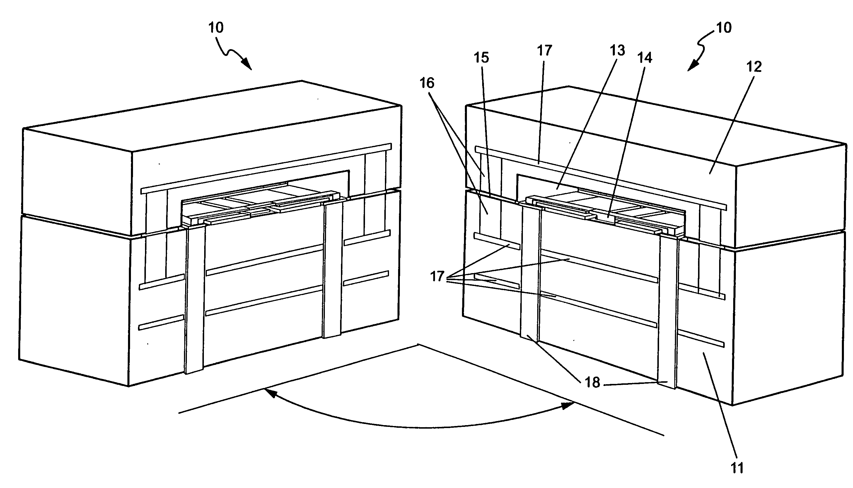
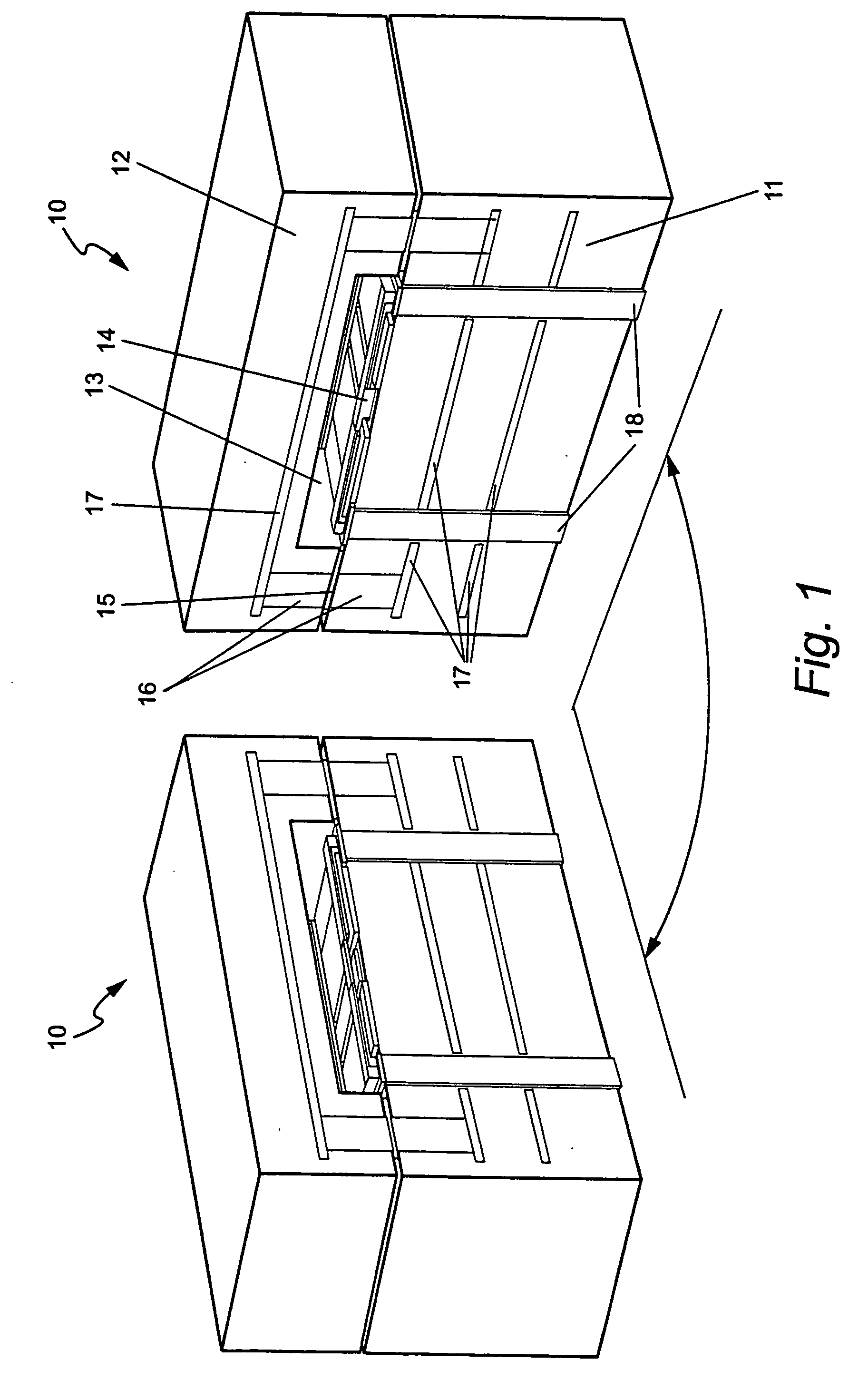
[0072]FIG. 1 shows two perspective views of a sliced open generalized MEMS RF device or system (“module”) 10 fabricated on a stack of multiple layers of an LTCC material which serve as a substrate 11 for a fabricated MEMS RF device 14. FIG. 1 also illustrates the packaging of the MEMS RF device wherein a cavity 13 is formed in a stack of LTCC layers 22 which are mated together to form a second substrate 12. The two substrates are then bonded or affixed together so as to enclose the MEMS RF device 14 within the cavity formed 13 in the upper LTCC substrate 12 prior to bonding the two LTCC substrates together to form device 10.

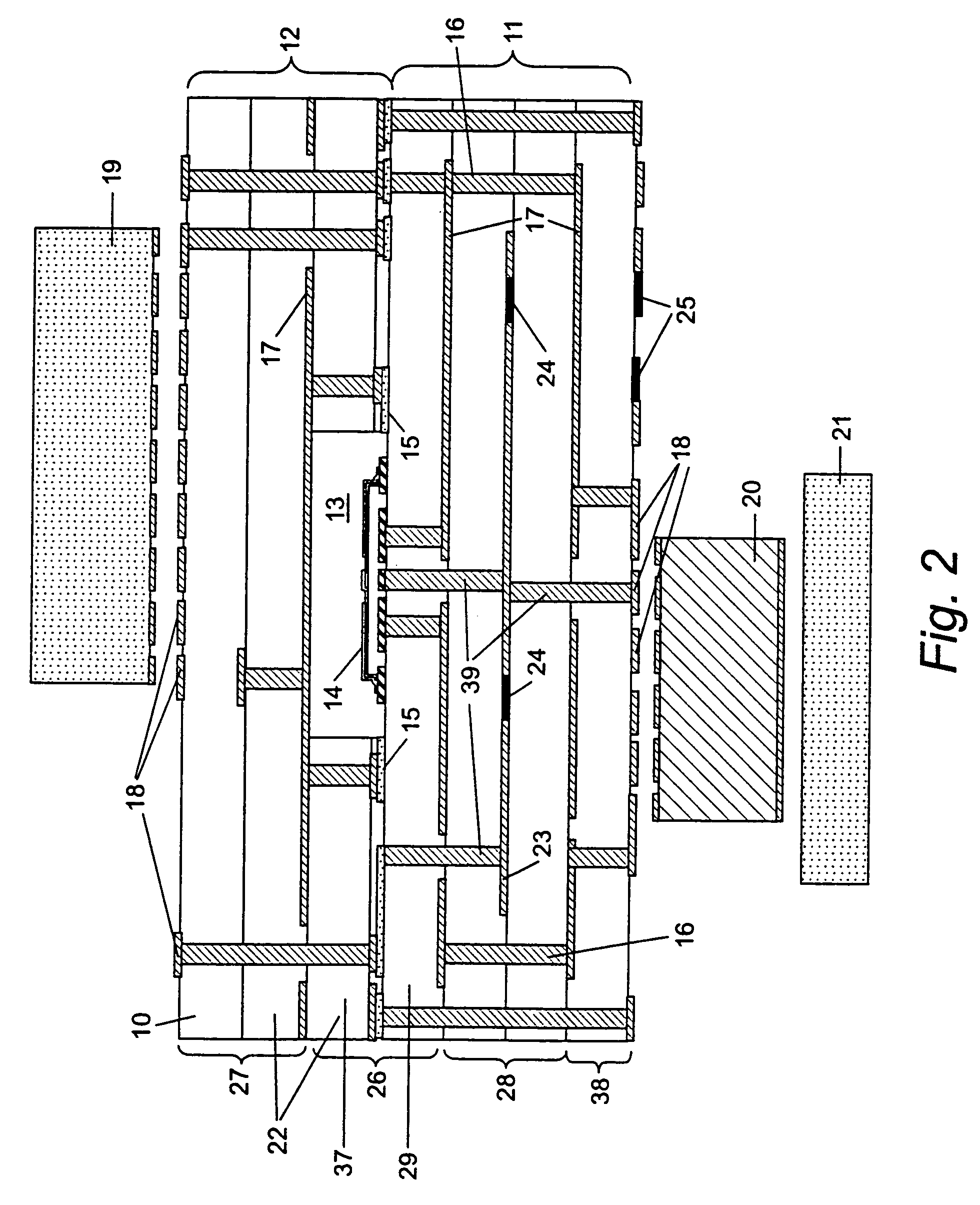
[0073]FIG. 2 illustrates a cross-sectional view of the preferred embodiment of a single generalized MEMS RF device 10 fabricated on a stack of multiple layers of LTCC material 22 and demonstrates the ability of providing suitable electrical connections 16 and 39 through a multiplicity of layers of the LTCC substrate 11 as well as the ability to form electrical c...


PUM

PropertyMeasurementUnit
temperatureaaaaaaaaaa
diameteraaaaaaaaaa
diameteraaaaaaaaaa

Abstract

A phased-array antenna system and other types of radio frequency (RF) devices and systems using microelectromechanical switches (“MEMS”) and low-temperature co-fired ceramic (“LTCC”) technology and a method of fabricating such phased-array antenna system and other types of radio frequency (RF) devices are disclosed. Each antenna or other type of device includes at least two multilayer ceramic modules and a MEMS device fabricated on one of the modules. Once fabrication of the MEMS device is completed, the two ceramic modules are bonded together, hermetically sealing the MEMS device, as well as allowing electrical connections between all device layers. The bottom ceramic module has also cavities at the backside for mounting integrated circuits. The internal layers are formed using conducting, resistive and high-k dielectric pastes available in standard LTCC fabrication and low-loss dielectric LTCC tape materials.

Description

FIELD OF THE INVENTION [0001] The present invention relates to Radio Frequency (RF) Micro-electro-mechanical systems (MEMS) and devices that are fabricated on or within Low-Temperature Co-Fired Ceramic (“LTCC”) substrates. The present invention also relates to a method of fabricating, integrating and packaging such MEMS RF devices and systems using MEMS and LTCC technologies. BACKGROUND OF THE INVENTION [0002] Microelectromechanical systems (MEMS) have been shown to be useful for a variety of consumer, industrial and military applications. Most MEMS devices are fabricated on semiconductor substrates (e.g., silicon, Gallium Arsenide, Silicon-On-Insulator, etc.) using standard Integrated Circuit (IC) processes in combination with specialized micromachining processes. Collectively these manufacturing technologies are frequently called microfabrication processes. [0003] Conventional MEMS processes which are performed on silicon or other semiconductor substrates can lower the cost of pro...

Claims


Application Information

Patent Timeline
Patent Type & Authority Applications(United States)
IPC IPC(8): H01H59/00H01P1/12H01P1/18H01Q1/38H01Q3/26H01Q15/00H01Q21/00H05K1/03H05K1/16
CPCB81B7/0064H01G5/16B81B2207/015B81B2207/092B81B2207/095B81B2207/096B81C2203/0118B81C2203/035B82Y30/00H01H59/0009H01H2057/006H01H2059/0072H01P1/127H01P1/184H01Q1/38H01Q3/26H01Q21/0087H05K1/0306H05K1/16H01Q15/0013H01Q15/004H01G5/18H01G5/40B81B2201/016H01L2224/16225H01L2924/15153B81B2207/07
Inventor HUFF, MICHAEL A.OZGUR, MEHMET
Owner FOR NAT RES INITIATIVES
Why Eureka
Try Eureka