Semiconductor module

a technology of semiconductor modules and memory, applied in the direction of semiconductor/solid-state device details, cross-talk/noise/interference reduction, instruments, etc., can solve the problems of unnecessarily changing the bus bus during access operation, data processor becoming an unnecessarily high-frequency noise source, and high-speed operation. high-speed noise resistance performance, high external noise resistance performan

Inactive Publication Date: 2005-08-04
HITACHI LTD
View PDF10 Cites 13 Cited by
  • Summary
  • Abstract
  • Description
  • Claims
  • Application Information

AI Technical Summary

Benefits of technology

[0042] In accordance with the above construction, the second semiconductor device such as a multichip module can relax a high frequency noise and can be operated at high speed, and has high external noise resisting performance and high reliability as the entire electronic circuit, and these contents can be realized at comparatively low cost.

Problems solved by technology

There is a case in which a print substrate (which is a printed circuit board and is hereinafter called PCB) mounting the SDRAM and the data processor often becomes an unneglectable high frequency noise source.
However, it is difficult to form the print substrate of predetermined desirable performance and manufacture cost of the print substrate is extremely increased when the entire print substrate is set to the multilayer wiring structure.
Firstly, it is necessary to sufficiently prevent memory data from being broken by a high frequency noise during the high speed operation of a memory.
However, in this construction, when a noise due to a high frequency wave flows-in through a bus connected to the memory and the microprocessor, read data or write data of the memory during an access operation are undesirably changed on the bus.
Secondly, it is necessary to consider the mounting layout of a device and the functional allocation of an external connecting electrode.
Thirdly, it is necessary to reduce a process number for mounting and assembling the devices into the multilayer wiring substrate so as not to reduce yield and reliability of the semiconductor module when the mounting layout of the devices of several kinds to the module substrate is determined.
However, in these publicly known examples, there is no description about the above room for further consideration.

Method used


Image

  • Semiconductor module
  • Semiconductor module
  • Semiconductor module

Examples


Embodiment Construction

>

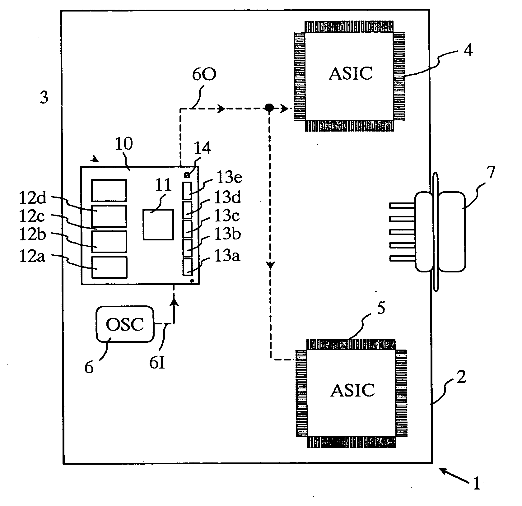
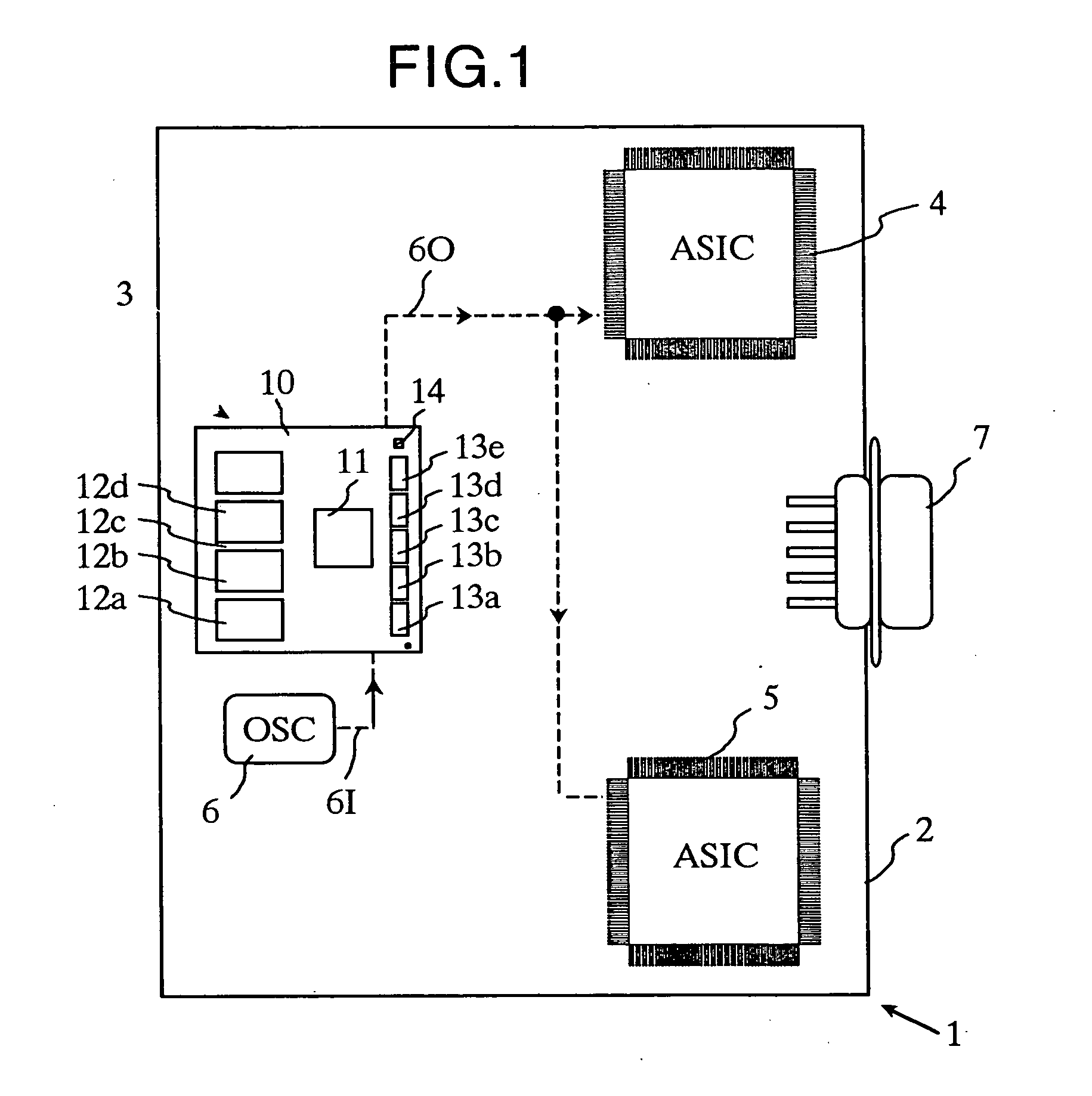
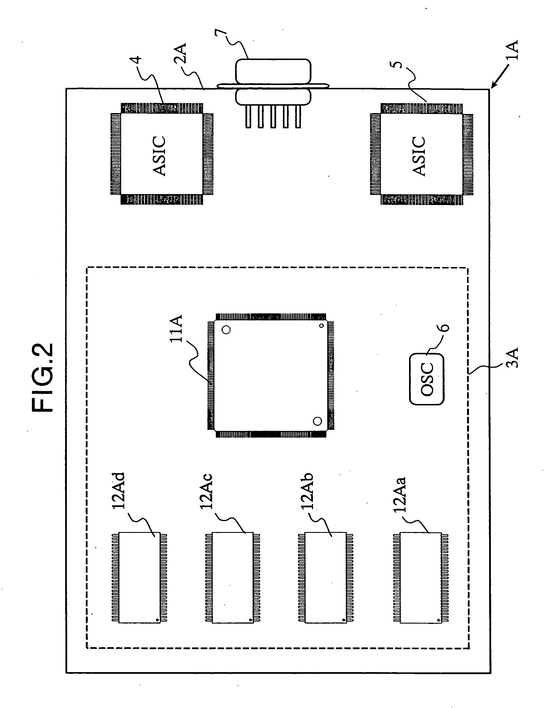
[0065]FIG. 1 shows one example of an electronic circuit in the present invention using a multichip module. The electronic circuit 1 shown in this figure is not particularly limited, but is a circuit in which a circuit portion requiring high speed data processing such as image processing and a circuit portion requiring no very high speed operation for realizing a communication function and a monitoring function of a system are mixed and mounted as in a digital copying machine, a car navigation device, etc.

[0066] In the electronic circuit 1 shown in FIG. 1, a multichip module 3 as a semiconductor module, ASICs (Application Specified ICs: ICs for a specific use) 4, 5 and a crystal oscillator (OSC) 6 are mounted to a wiring pattern in which the illustration of a wiring substrate 2 is omitted. An input / output connector 7 is connected to the predetermined wiring pattern omitting the illustration of the wiring substrate 2 so that the electronic circuit 1 can be connected to another devic...


PUM


Abstract

A high speed operating circuit such as a data processor chip and memory chips constituting an electronic circuit is mounted to a multilayer wiring substrate in the state of a bare chip, and is set to a multichip module. This multichip module is mounted to a wiring substrate constituting the electronic circuit. In the multichip module, buffer circuits are inserted into a module internal bus commonly connected to the data processor chip and the memory chips. The buffer circuits are set to an address output buffer, a control signal output buffer and a data input/output buffer set to a high impedance state in accordance with an operating selection of the memory chips. When high frequency noise resisting characteristics are strengthened by the multilayer wiring substrate and the data processor chip gets access to the memory chips, an external noise tends to flow into a memory through the module internal bus connected to the data processor chip and the memory chips. However, the buffer circuits restrain the flow-in of such an external noise and prevent memory data from being broken by the high frequency noise during a memory access operation.

Description

BACKGROUND OF THE INVENTION [0001] 1. Field of the Invention [0002] The present invention relates to a semiconductor module mounting plural semiconductor integrated circuit chips thereto, and relates to an effective technique applied to a multichip module in which a data processor chip and a memory chip are mounted to e.g., a multilayer wiring substrate. [0003] 2. Background Art [0004] An electronic circuit for performing image processing, etc. is constructed by a data processor called a microprocessor or a microcomputer, etc., and a high speed operating memory represented by a synchronous DRAM (hereinafter called SDRAM), etc. accessed by the data processor in many cases. A high speed operation such as a 100 MHz operation and a 133 MHz operation represented by standards of “PC100”, “PC133”, etc. is further required in the recent SDRAM. When the high speed operation must be performed by including the high speed operating memory of this kind, etc. in the electronic circuit, it is also...

Claims


Application Information

Patent Timeline
Patent Type & Authority Applications(United States)
IPC IPC(8): G11C5/00G11C5/06H05K1/02H05K1/14
CPCG11C5/005G11C5/04G11C5/06H01L23/50H01L2224/16225H01L25/16H01L2924/3011H05K1/0216H05K1/141H01L23/552
Inventor SUGITA, NORIHIKOKIKUCHI, TAKAFUMIMIYASHITA, KOICHIIKEGAMI, HIKARU
Owner HITACHI LTD
Why Eureka
Try Eureka