III-nitride light emitting device with reduced polarization fields

a technology of polarization field and light emitting device, which is applied in the direction of solid-state devices, lasers, semiconductor lasers, etc., can solve the problems of reducing efficiency, reducing probability, and reducing efficiency, so as to avoid inefficiencies caused, reduce the polarization field

Active Publication Date: 2005-08-04
LUMILEDS
View PDF2 Cites 19 Cited by
  • Summary
  • Abstract
  • Description
  • Claims
  • Application Information

AI Technical Summary

Benefits of technology

[0012] Matching the net polarization in the spacer layers and the light emitting layers may move polarization-induced sheet charges away from the interfaces between the spacer layers and the light emitting layer to the interface between the p- and n-type regions and the spacer layers. Once the sheet-charges are spaced apart from the light emitting layer, in some embodiments the interface between the p- and n-type regions and the spacer layers is doped, which may reduce the polarization field across the light emitting layer. Accordingly, matching the net polarization in the spacer layers and the light emitting layers, and canceling sheet charges by doping may avoid the inefficiencies caused by polarization, described above.

Problems solved by technology

When the device is operating, the naturally occurring polarization field generated by σ1 and σ2 reduces the efficiency in a number of ways.
This spatial separation of free carriers lowers the probability of radiative recombination, reducing emission efficiency.

Method used


Image

  • III-nitride light emitting device with reduced polarization fields
  • III-nitride light emitting device with reduced polarization fields
  • III-nitride light emitting device with reduced polarization fields

Examples


Embodiment Construction

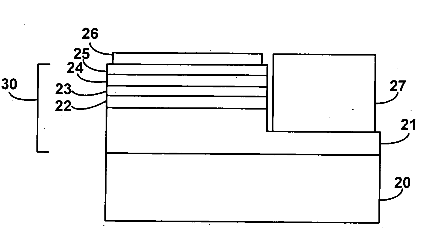
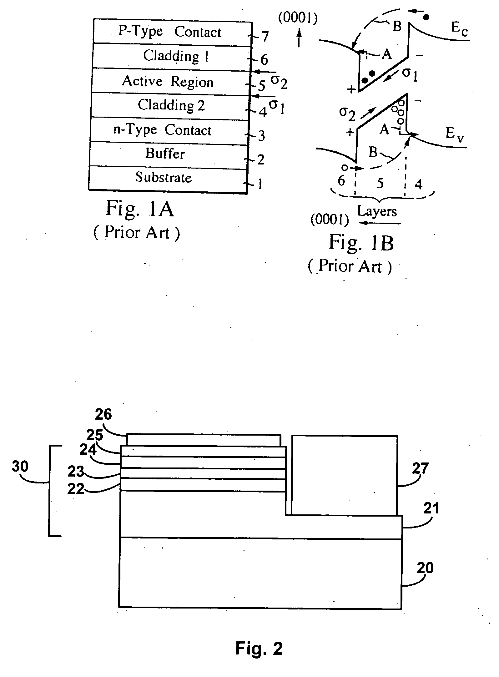
[0021]FIG. 2 illustrates a device according to several embodiments of the invention. An n-type region 21 is formed over a suitable substrate 20, usually sapphire, SiC, or GaN. Active region 23 is sandwiched between two spacer layers, an n-type spacer layer 22 and a p-type spacer layer 24. Active region 23 may be a single light emitting layer or may include one or more quantum well layers separated by barrier layers. A p-type region 25 is formed over p-type spacer layer 24. P-contact 26 provides electrical contact to the p-side of the active region and n-contact 27 provides electrical contact to the n-side of the active region. Two possible arrangements of the p- and n-contacts are described below in FIGS. 7-10.

[0022] In some embodiments of the invention, one or more of p-type spacer layer 24, n-type spacer layer 22, and the barrier layers separating the quantum wells in a multiple quantum well active region may be quaternary alloys of aluminum, indium, gallium, and nitrogen. The co...


PUM


Abstract

A semiconductor light emitting device includes a light emitting layer sandwiched between two spacer layers. The difference between the net polarization in at least one of the spacer layers and the net polarization in the light emitting layer is less than in the device with conventional spacer layers, such as GaN spacer layers. The difference between the net polarization in at least one of the spacer layers and the net polarization in the light emitting layer is less than about 0.02 C / m2. In some embodiments, at least one of the spacer layers is a quaternary alloy of aluminum, indium, gallium, and nitrogen.

Description

BACKGROUND [0001] 1. Field of Invention [0002] The present invention relates to III-nitride light emitting devices. [0003] 2. Description of Related Art [0004] Semiconductor light-emitting devices including light emitting diodes (LEDs), resonant cavity light emitting diodes (RCLEDs), vertical cavity laser diodes (VCSELs), and edge emitting lasers are among the most efficient light sources currently available. Materials systems currently of interest in the manufacture of high-brightness light emitting devices capable of operation across the visible spectrum include Group III-V semiconductors, particularly binary, ternary, and quaternary alloys of gallium, aluminum, indium, and nitrogen, also referred to as III-nitride materials. Typically, III-nitride light emitting devices are fabricated by epitaxially growing a stack of semiconductor layers of different compositions and dopant concentrations on a sapphire, silicon carbide, III-nitride, or other suitable substrate by metal-organic c...

Claims


Application Information

Patent Timeline
Patent Type & Authority Applications(United States)
IPC IPC(8): H01L33/32
CPCH01L33/32
Inventor WATANABE, SATOSHISTOCKMAN, STEPHEN A.
Owner LUMILEDS
Why Eureka
Try Eureka