LED epitaxial growth method suitable for 4-inch substrate

An epitaxial growth and substrate technology, applied in the direction of electrical components, circuits, semiconductor devices, etc., can solve the problems of uneven growth of materials in the chip, low product yield, low luminous efficiency, and large warping of epitaxial wafers, etc., to improve luminous efficiency And antistatic ability, antistatic and other performance improvement, improve the effect of crystal quality

Active Publication Date: 2019-06-07
XIANGNENG HUALEI OPTOELECTRONICS
View PDF5 Cites 0 Cited by
  • Summary
  • Abstract
  • Description
  • Claims
  • Application Information

AI Technical Summary

Problems solved by technology

After the LED size is upgraded to 4 inches, LEDs generally have technical problems such as large warping of epitaxial wafers and low luminous efficiency. Therefore, how to grow better epitaxial wafers has attracted increasing attention.
[0003] In the existing epitaxial growth technology, there is a common problem of large warping of the epitaxial wafer, especially when the epitaxial crystal is grown on a 4-inch sapphire substrate, due to the lattice mismatch, the polarization field generated during the epitaxial growth process, and the material in the wafer Uneven growth and other problems make the epitaxial wafer warp more, and the product yield and luminous efficiency are lower

Method used


Image

  • LED epitaxial growth method suitable for 4-inch substrate
  • LED epitaxial growth method suitable for 4-inch substrate
  • LED epitaxial growth method suitable for 4-inch substrate

Examples


Embodiment 1

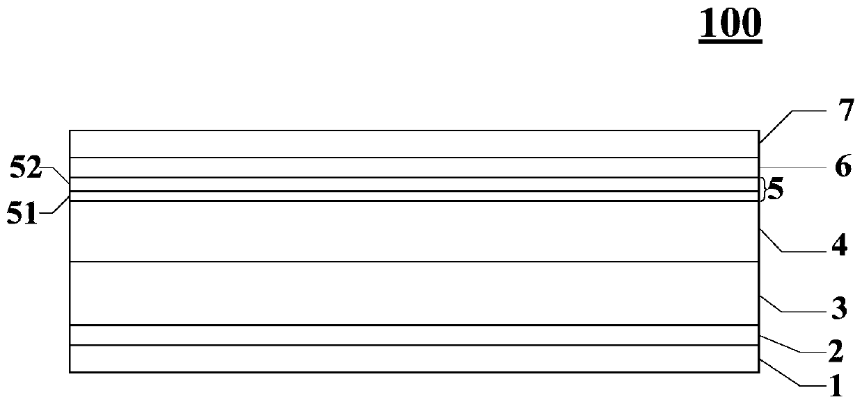
[0057] figure 1 Shown is a schematic structural diagram of an LED epitaxial layer 100 in the prior art. The LED epitaxial layer 100 in the prior art includes: a substrate 1, a low-temperature buffer layer 2, an undoped GaN layer 3, and Si-doped n-type GaN Layer 4, active layer MOW 5, P-type AlGaN layer 6, magnesium-doped P-type GaN layer 7; wherein, the active layer MOW 5 includes In y1 Ga (1-y1) N layer 51 and GaN layer 52 .

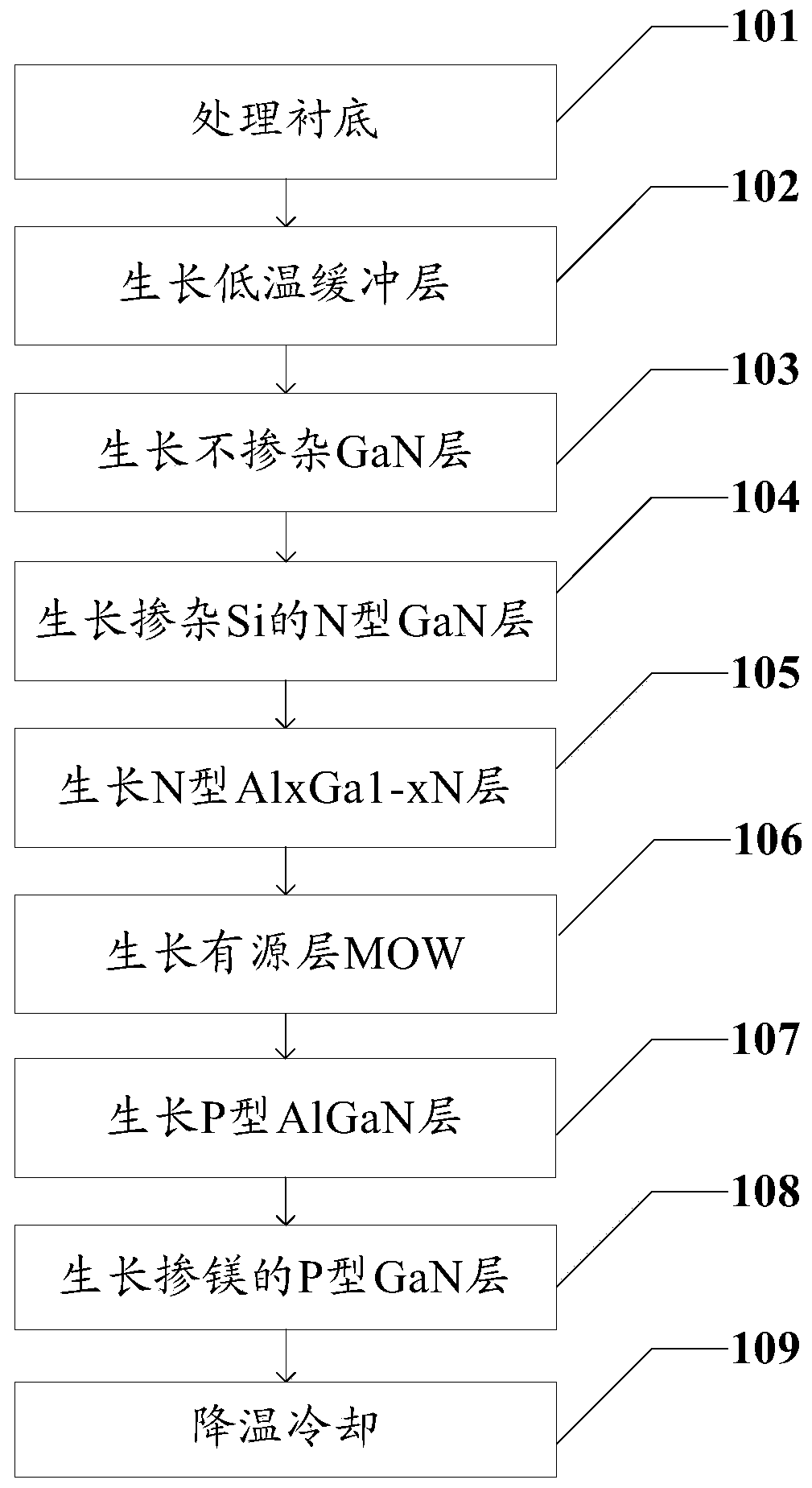
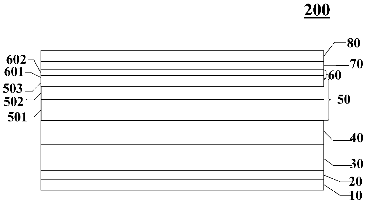
[0058] figure 2 Shown is a flow chart of an LED epitaxial growth method suitable for a 4-inch substrate provided by the embodiment of the present application, image 3 Shown is a schematic structural diagram of the LED epitaxial layer 200 in the embodiment of the present application, please refer to figure 2 and image 3 , the embodiment of the present application provides an LED epitaxial growth method suitable for a 4-inch substrate, including:

[0059] Step 101, processing the substrate 10;

[0060] Step 102, growing a low-temperature buffer...

Embodiment 2

[0098] Please combine figure 1 , the LED epitaxial layer growth method in the prior art includes: processing the substrate 1, growing a low-temperature buffer layer 2, growing an undoped GaN layer 3, growing an n-type GaN layer 4 doped with Si, growing an active layer MOW 5, growing P-type AlGaN layer 6, growth of magnesium-doped P-type GaN layer 7, epitaxial layer structure, please refer to figure 1 . The embodiment of the present application adds N-type Al on the basis of the prior art x Ga 1-x N layer 50. In this embodiment, 1000 pieces of sample 1 are prepared according to the LED epitaxial growth method in the prior art, and 1000 pieces of sample 2 are prepared according to the LED epitaxial growth method of the present application. After the samples were grown, 4 samples each of sample 1 and sample 2 were randomly selected, and the XRD102 surface of the epitaxial wafer was tested under the same conditions. Please refer to Table 1. Table 1 shows the epitaxial XRD test...


PUM


Abstract

The invention discloses an LED epitaxial growth method suitable for a 4-inch substrate, and relates to the technical field of LEDs. The LED epitaxial growth method comprises the steps of: processing asubstrate, growing a low-temperature buffer layer, growing an undoped GaN layer, growing a Si-doped N-type GaN layer, growing an N-type AlxGa1-xN layer, growing an active layer MOW, growing a P-typeAlGaN layer, growing a magnesium-doped P-type GaN layer, and performing cooling. The N-type AlxGa1-xN layer is introduced and the Si dosage concentration regular gradual change in the growth process is controlled to facilitate elimination of the stress accumulative effect of the 4-inch sapphire substrate on a GaN film and obviously increase a stress control window of the epitaxial film material soas to reduce the warping of the epitaxial wafer, facilitate improvement of the qualified rate of the GaN epitaxial wafer and improve the luminous efficiency and antistatic capability of the LED.

Description

technical field [0001] The invention relates to the technical field of LEDs, in particular to an LED epitaxial growth method suitable for a 4-inch substrate. Background technique [0002] LED (Light Emitting Diode, Light Emitting Diode) is a kind of solid-state lighting. Due to the advantages of LED, such as small size, low power consumption, long service life, high brightness, environmental protection, and durability, it is recognized by consumers, and the scale of domestic LED production is also increasing. Gradually expanding, and the size of LEDs produced by most manufacturers has been upgraded from 2 inches to 4 inches. After the LED size is upgraded to 4 inches, LEDs generally have technical problems such as large warping of epitaxial wafers and low luminous efficiency. Therefore, how to grow better epitaxial wafers has attracted increasing attention. [0003] In the existing epitaxial growth technology, there is a common problem of large warping of the epitaxial wafe...

Claims


Application Information

Patent Timeline
Patent Type & Authority Applications(China)
IPC IPC(8): H01L33/00
Inventor 徐平季辉吴奇峰
Owner XIANGNENG HUALEI OPTOELECTRONICS
Why Eureka
Try Eureka