Vertical GaN light emitting diode and method for manufacturing the same

a technology of light-emitting diodes and vertical gans, which is applied in the direction of basic electric elements, electrical equipment, semiconductor devices, etc., can solve the problems of limiting the structure of gan light-emitting diodes, and no practical technique for forming bulk single crystals of gan, so as to improve the current density distribution

Inactive Publication Date: 2005-08-11
SAMSUNG ELECTRONICS CO LTD
View PDF6 Cites 94 Cited by
  • Summary
  • Abstract
  • Description
  • Claims
  • Application Information

AI Technical Summary

Benefits of technology

[0021] Moreover, preferably, the first conductive GaN clad layer may be a GaN crystalline layer doped with an n-type impurity, and the second conductive GaN clad layer may be an GaN crystalline layer doped with a p-type impurity, so as to enhance the current density distribution.

Problems solved by technology

The same as other Group III nitride semiconductor materials for emitting blue light, there is no practical technique for forming a bulk single crystal made of GaN.
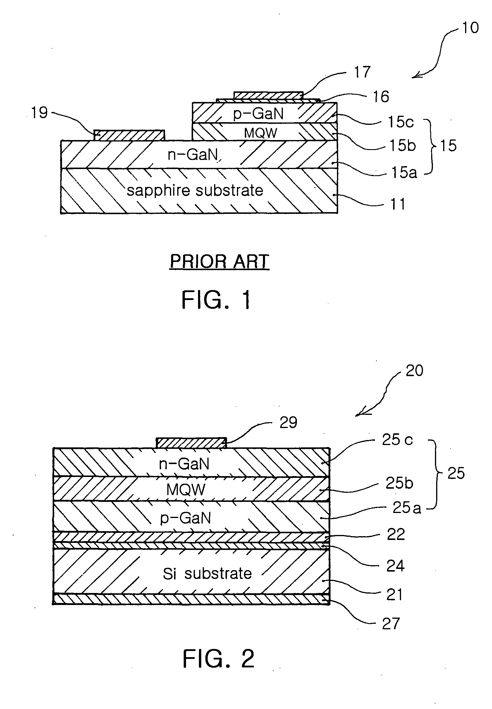
However, a sapphire substrate has an insulating property, thus limiting the structure of a GaN light emitting diode.

Method used


Image

  • Vertical GaN light emitting diode and method for manufacturing the same
  • Vertical GaN light emitting diode and method for manufacturing the same
  • Vertical GaN light emitting diode and method for manufacturing the same

Examples


Embodiment Construction

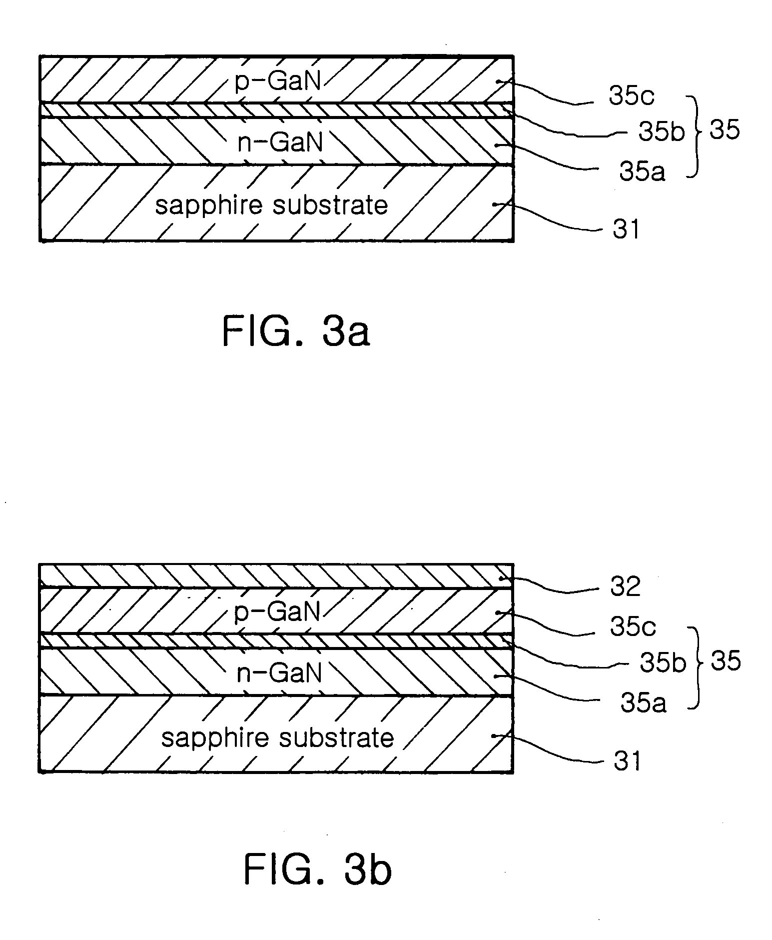
[0032] Now, preferred embodiments of the present invention will be described in detail with reference to the annexed drawings.

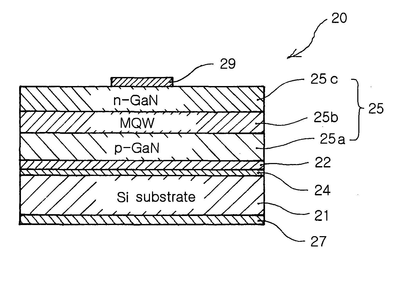
[0033]FIG. 2 is a cross-sectional view of a vertical GaN light emitting diode 20 in accordance with one preferred embodiment of the present invention.

[0034] The vertical GaN light emitting diode 40 comprises a light emitting structure 25 including a p-type GaN clad layer 25a, an active layer 25b, and an n-type GaN clad layer 25c. Further, the GaN light emitting diode 40 selectively comprises a reflective layer 22 formed on the lower surface of the p-type GaN clad layer 25a. The reflective layer 22 is attached to a silicon substrate 21 using a conductive adhesive layer 24. The reflective layer 22 serves to improve the effective luminance depending on light emitted from the upper surface of the GaN light emitting diode 20, and is made of a metal with high reflectivity. Preferably, the reflective layer 22 is made of a material selected from the group consistin...


PUM


Abstract

Disclosed are a vertical GaN light emitting diode and a method for manufacturing the same. The vertical GaN light emitting diode comprises a first conductive GaN clad layer with an upper surface provided with a first contact formed thereon, an active layer formed on a lower surface of the first conductive GaN clad layer, a second conductive GaN clad layer formed on a lower surface of the active layer, a conductive adhesive layer formed on the second conductive GaN clad layer, and a conductive substrate, with a lower surface provided with a second contact formed thereon, formed on a lower surface of the conductive adhesive layer. The method for manufacturing the vertical GaN light emitting diodes comprises the step of removing the sapphire substrate from the light emitting structure so as to prevent the damages on a GaN single crystal plane of the structure.

Description

BACKGROUND OF THE INVENTION [0001] 1. Field of the Invention [0002] The present invention relates to a vertical GaN light emitting diode and a method for manufacturing the same, and more particularly to a vertical GaN light emitting diode, from which an insulating sapphire substrate with low thermal conductivity is removed and in which a conductive substrate such as a silicon substrate is installed so as to improve the luminance and the reliability of the diode, and a method for manufacturing the vertical GaN light emitting diode. [0003] 2. Description of the Related Art [0004] Generally, light emitting diodes (LEDs) are semiconductor elements, which emit light based on the recoupling of electrons and holes, and are widely used as various types of light sources in optical communication and electronic equipment. GaN serves as a compound for manufacturing blue-light emitting diodes. [0005] Frequency (or wavelength) of light emitted from the light emitting diode is functionally related...

Claims


Application Information

Patent Timeline
Patent Type & Authority Applications(United States)
IPC IPC(8): H01L21/00H01L29/06H01L33/10H01L33/32H01L33/34
CPCH01L33/0079H01L2221/68363H01L33/32H01L33/0095H01L33/0093
Inventor PARK, YOUNG HOHAHM, HUN JOONA, JEONG SEOKYOO, SEUNG JIN
Owner SAMSUNG ELECTRONICS CO LTD
Why Eureka
Try Eureka