Current sense trench type MOSFET with improved accuracy and ESD withstand capability

a trench type, mosfet technology, applied in electrical devices, semiconductor devices, instruments, etc., can solve the problems of reducing the cell pitch, reducing difficult to produce current sensing mosfets with low sense ratio variation, etc., to reduce the yield of current sensing mosfet wafers, reduce the sense ratio variation, and reduce the cell pitch. , the effect of low cell pitch

Active Publication Date: 2005-08-11
INFINEON TECH AMERICAS CORP
View PDF4 Cites 9 Cited by
  • Summary
  • Abstract
  • Description
  • Claims
  • Application Information

AI Technical Summary

Benefits of technology

[0011] In accordance with a first feature of the invention, and to reduce current sense ratio variation, current conduction through the periphery of the active area of the trench sense die is reduced.
[0015] Thus, sense ratio variation due to fabrication steps, especially in a trench MOSFET, and with low cell pitch devices, is reduced. Important benefits include reduced sense ratio variation in fabrication lots and over different gate voltages.
[0018] The important benefit of this aspect of the invention is improved ESD withstand capability of a current sensing MOSFET without additional processing steps.

Problems solved by technology

Because the amount of current conducted in the peripheral region is subject to variation due to a number of processing or manufacturing steps, it is difficult to produce current sense MOSFETs with low sense ratio variation.
Moreover, reducing the cell pitch poses increased challenges in controlling sense ratio variation.
Electrostatic discharge destruction of a MOSFET occurs when the voltage across two pins induced by static charge is high enough to damage the dielectric thin film of the device.
The yield of a current sensing MOSFET wafers is often decreased due to ESD damage.
ESD destruction of the device is also a reliability risk.

Method used


Image

  • Current sense trench type MOSFET with improved accuracy and ESD withstand capability
  • Current sense trench type MOSFET with improved accuracy and ESD withstand capability
  • Current sense trench type MOSFET with improved accuracy and ESD withstand capability

Examples


Embodiment Construction

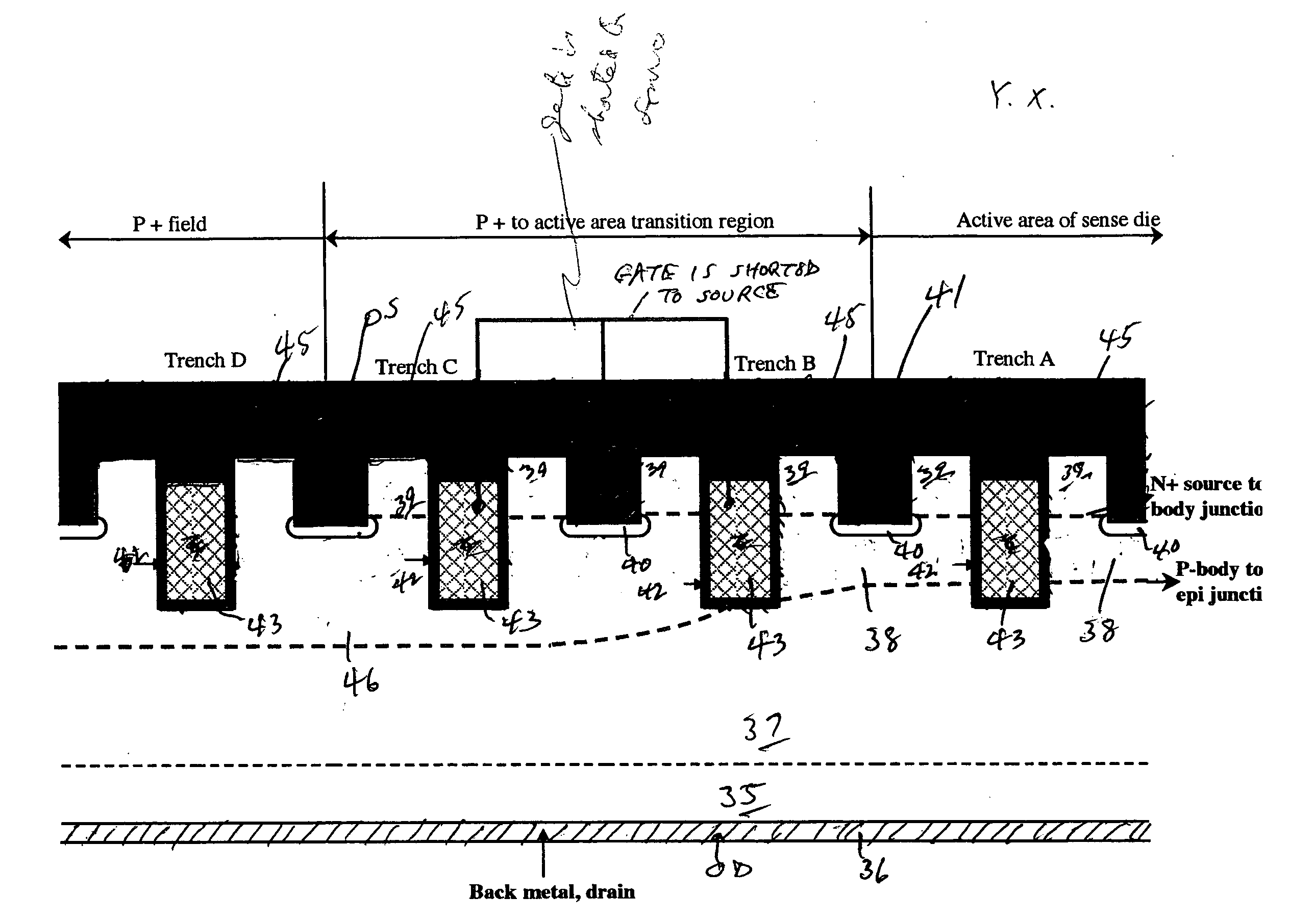
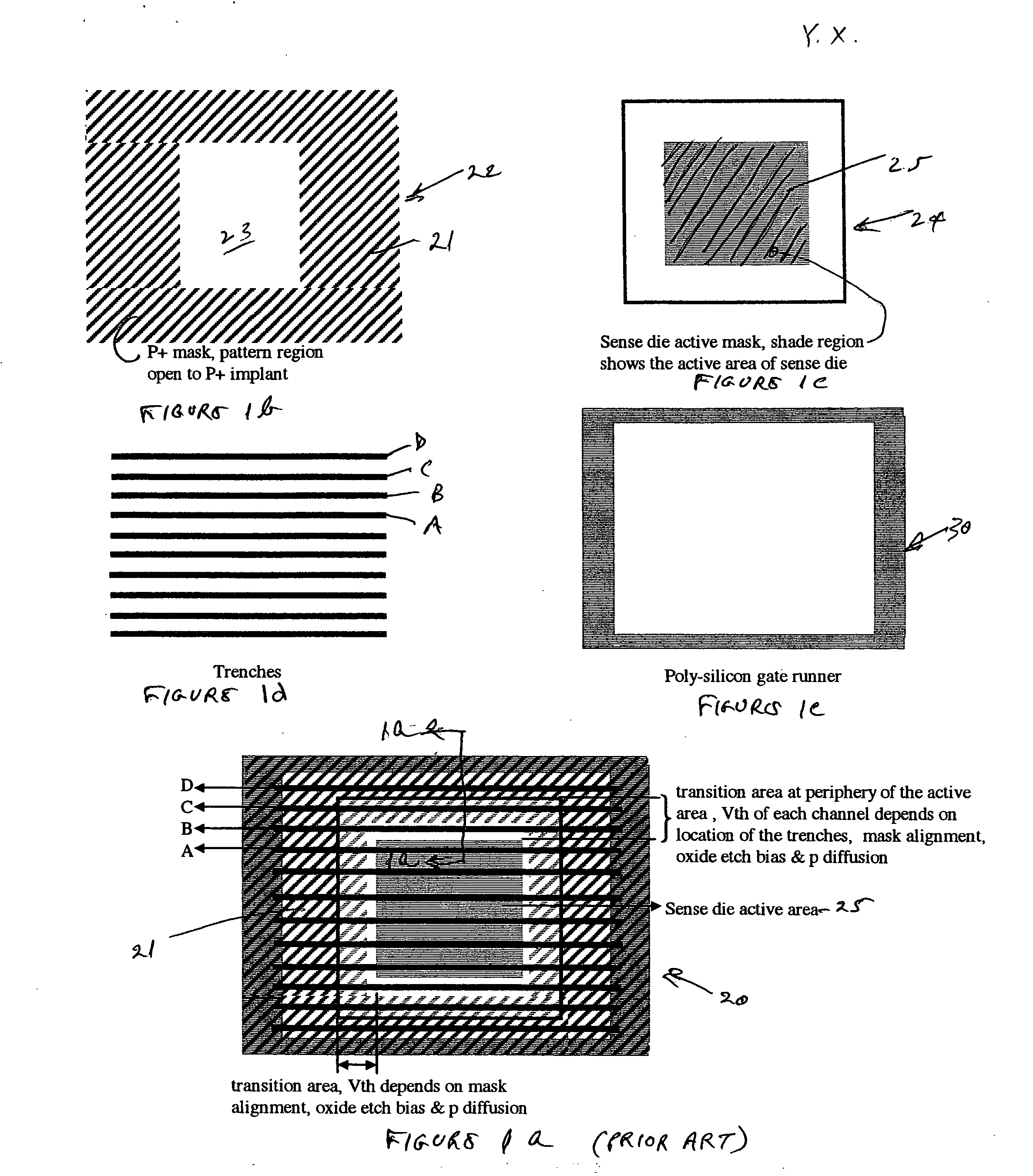
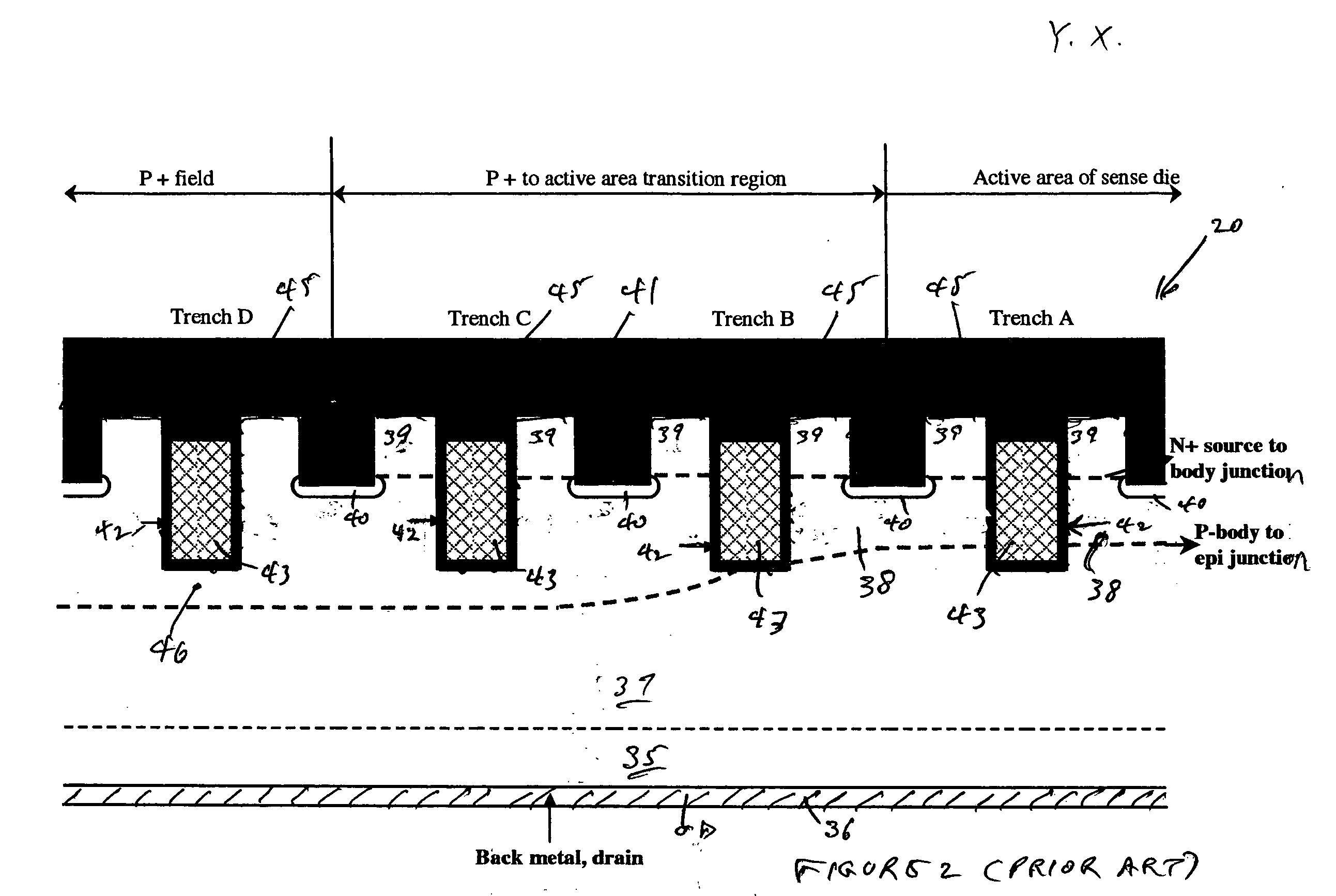
[0038]FIG. 1a is a top view of a prior art sense die design 20. The sense die is shown as an N channel device, but it is to be understood that it can be a P channel device with all conductivity types reversed from those described. The active area 25 of the sense die 20 is isolated from the main FET by a P+ region 21 defined by the P+ mask 22 of FIG. 1b. The P+ mask 22 defines an open area 23 in the field oxide for boron implantation. The P+ mask has a certain overlap with the active mask 24 (FIG. 1c) that defines the open area for channel and source implantation. The active area 25 of the sense die 20 is inside the active mask 24. The periphery of active area 25 constitutes the transition from active area to the P+ field 21.

[0039] In the example shown in FIG. 1a, trench A FIG. 1d is located at the active area 25, trenches B and C are located at the transition region from active area 25 to the P+ field 21, and trench D is located at the P+ field 21 without overlap with the active ma...


PUM

PropertyMeasurementUnit
active areaaaaaaaaaaa
areaaaaaaaaaaa
areaaaaaaaaaaa

Abstract

The active area of a current sense die is surrounded by a transition region which extends to the terminating periphery of the die. Spaced parallel MOSgated trenches extend through and define an active area. The trench positions in the transition region are eliminated or are deactivated, as by shorting to the MOSFET source of the trench, or by removing the source regions in areas of the transition region. By inactivating MOSgate action in the transition region surrounding the source, the device is made less sensitive to current ratio variation due to varying manufacturing tolerances. The gate to source capacitance is increased by surrounding the active area with an enlarged P+ field region which is at least five times the area of the active region, thereby to make the device less sensitive to ESD failure.

Description

RELATED APPLICATION [0001] This application claims the benefit of U.S. Provisional Application No. 60 / 540,747, filed Jan. 30, 2004 and U.S. Provisional Application No. 60 / 540,501, filed Jan. 30, 2004.FILED OF THE INVENTION [0002] This invention relates to semiconductor devices and processes for their manufacture and more specifically relates to current sense MOSFETs of a trench type topology and processes of their manufacture for improved accuracy (reduced sense ratio variation) and improved electrostatic discharge (ESD) withstand capability. BACKGROUND OF THE INVENTION [0003] A first feature of the present invention deals with the variation of the current sense ratio variation which is encountered in trench type current sense MOSFETs. [0004] In a current sensing MOSFET, a small fraction of the total active area of a power MOSFET is employed to sense the current through an independent source terminal. The current sense ratio is the ratio of current conducted through the main FET and...

Claims


Application Information

Patent Timeline
Patent Type & Authority Applications(United States)
IPC IPC(8): G11C5/02H01L29/06H01L29/08H01L29/10H01L29/40H01L29/417H01L29/423H01L29/78
CPCH01L29/0696H01L29/0847H01L29/1095H01L29/407H01L29/7815H01L29/4232H01L29/4238H01L29/7811H01L29/7813H01L29/41766
Inventor CAO, JIANJUNXIAO, YINGSPRING, KYLEKINZER, DANIEL M.
Owner INFINEON TECH AMERICAS CORP
Why Eureka
Try Eureka