Optical modulator

a modulator and optical technology, applied in the field of optical waveguide devices, can solve the problems of reducing the signal waveform after transmission, affecting the efficiency of optical modulators, so as to achieve the effect of suppressing the loss of radiation

Active Publication Date: 2005-08-11
FUJITSU LTD
View PDF2 Cites 34 Cited by
  • Summary
  • Abstract
  • Description
  • Claims
  • Application Information

AI Technical Summary

Benefits of technology

[0023] Furthermore, for the substrate of the optical modulator, it is preferable that the optical waveguide is formed on a surface of a Z-cut crystal substrate, and the surface on which the optical waveguide is formed, has a +Z face in the polarization inversed region and a −Z face in t

Problems solved by technology

In the case where the curved section is formed in the part of the optical waveguide, an optical loss (radiation loss) occurring in the curved section is a problem.
However, the above described conventional Mach-Zehnder type optical modulator has the following problems.
Thus, there is a problem in that when the signal is switched from “0” to “1” or from “1” to “0”, a wavelength change (wavelength chirp) in a modulated light occurs, which degrades the signal waveform after transmission.
However, since it is not possible to arrange the parallel waveguides directly below the signal electrode, there is a large distance between the signal electrode and the waveguides.
Therefore, there is a disadvantage in that a high drive voltage must be applied.
Therefore, there is a disadvantage in that the circuit structure of drive system becomes complicated.
In order to miniaturize the Mach-Zehnder type optical modulator, even if the curved section is formed in the part of the optical waveguide, and furthermore, the optical loss occurring in the curved section is suppressed using the above described technique of Japanese Unexamined Patent Publication No. 11-167032, it is difficult to reduce the curvature of the

Method used


Image

  • Optical modulator
  • Optical modulator
  • Optical modulator

Examples


Embodiment Construction

[0033] Hereunder is a description of embodiments of implementing an optical modulator of the present invention with reference to the appended figures. Here, identical reference numerals denote identical or equivalent parts throughout all of the drawings.

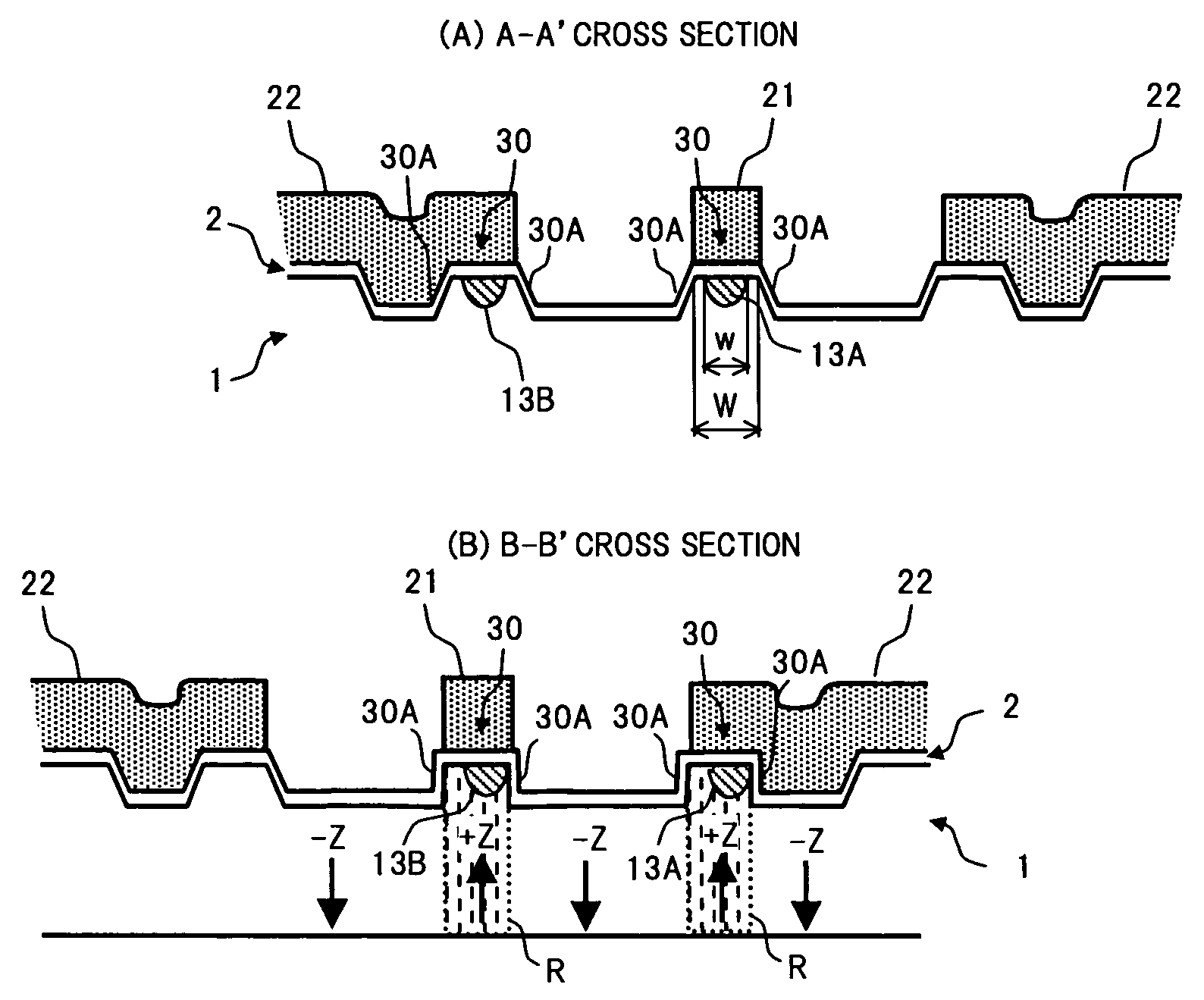
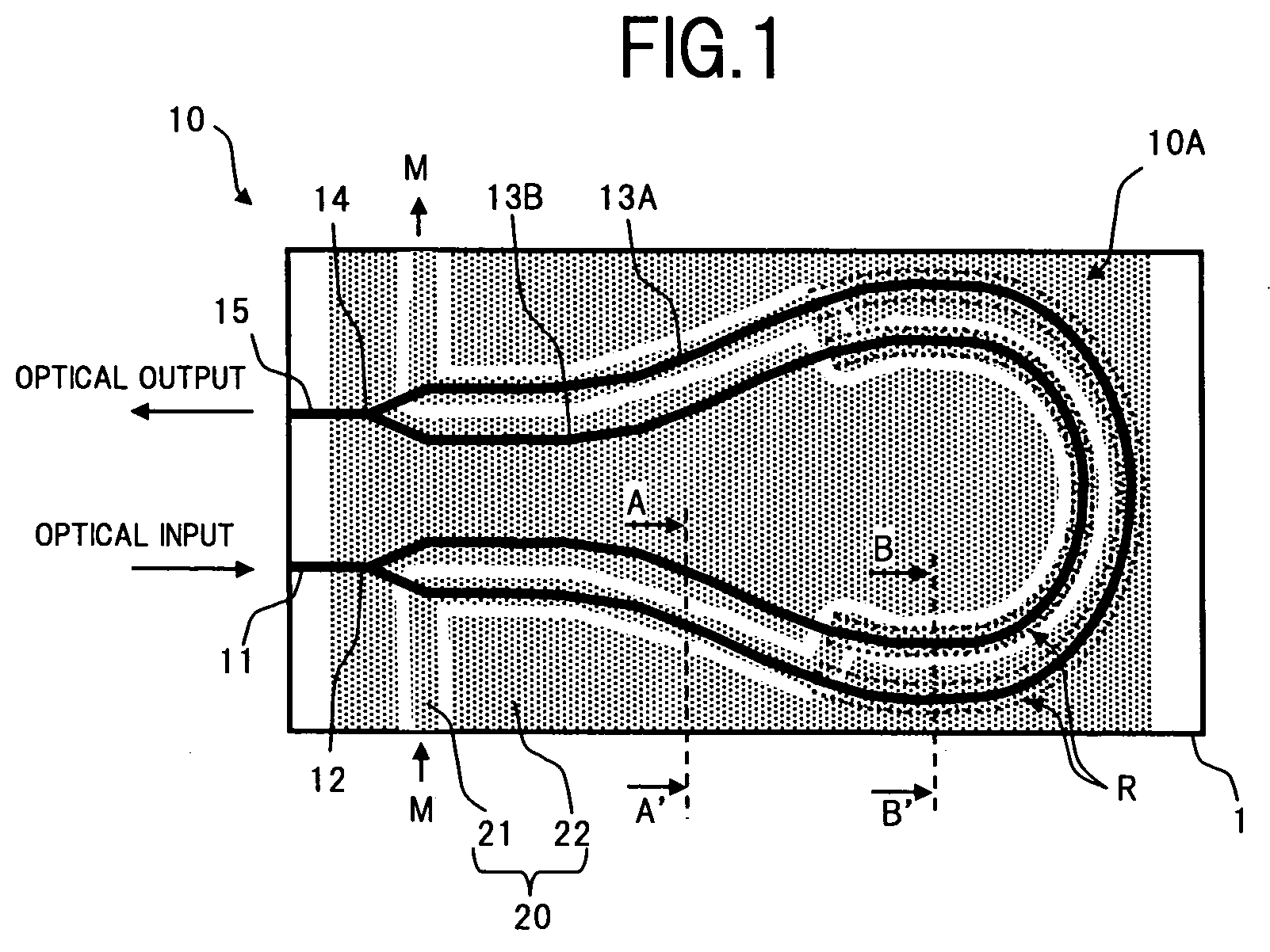
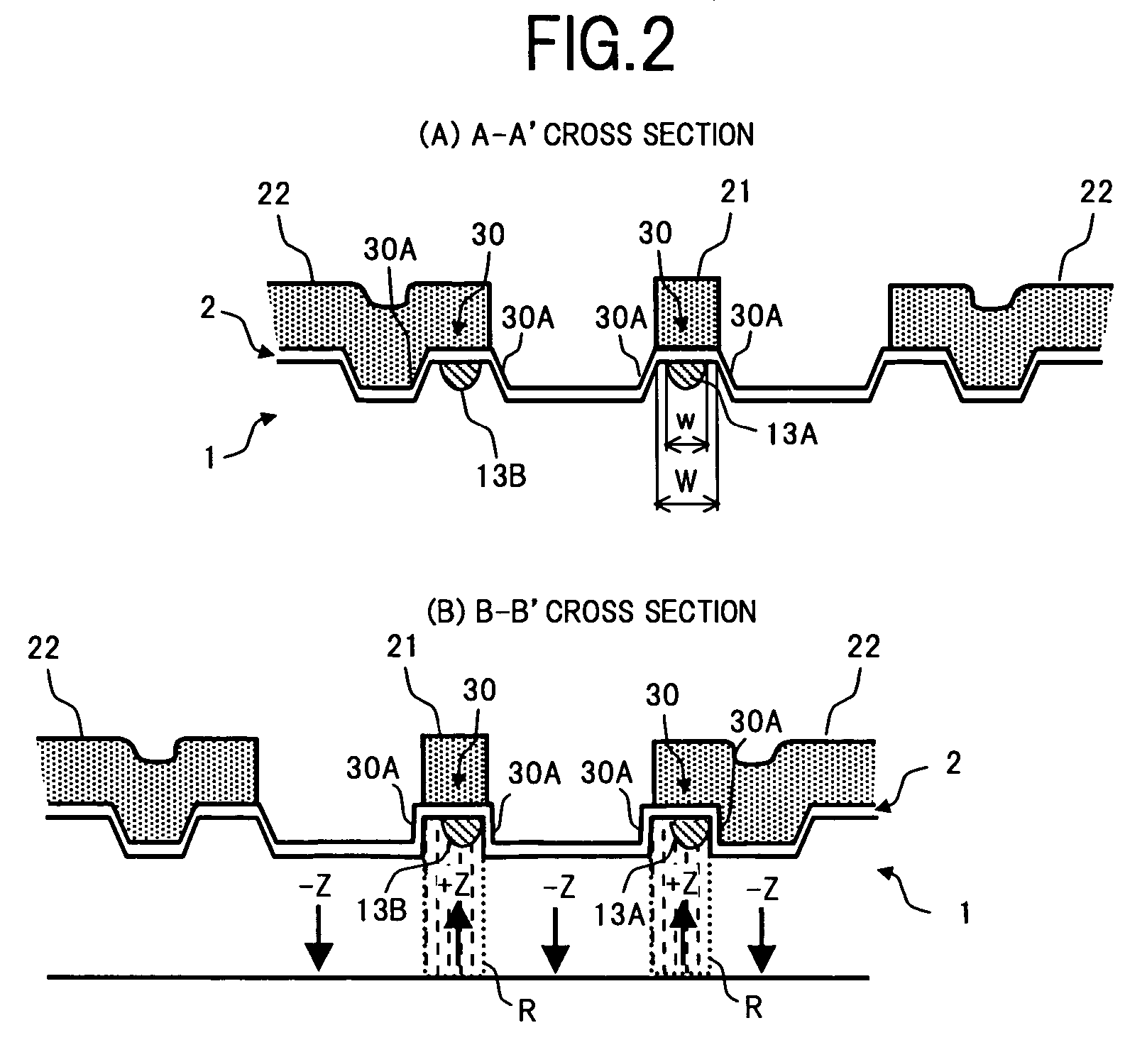
[0034]FIG. 1 is a plan view showing a configuration of a Mach-Zehnder type optical modulator according to an embodiment of the present invention. Further, FIG. 2 is a diagram showing main structures of cross-sections in respective sections of FIG. 1, where (A) is a cross-sectional diagram through A-A′, and (B) is a cross-sectional diagram through B-B′.

[0035] In FIG. 1 and FIG. 2, the Mach-Zehnder type optical modulator of the present embodiment comprises a substrate 1 having an electro-optical effect, an optical waveguide 10 formed on a surface of the substrate 1, and a coplanar electrode 20 formed on the surface of the substrate 1 via a buffer layer 2.

[0036] For the substrate 1, a Z-cut lithium niobate (LiNbO3) substrate, a lithi...


PUM


Abstract

An object of the invention is to provide a Mach-Zehnder type optical modulator that can reduce wavelength chirp occurring in a modulated light, and also can reduce an optical loss with a small sized configuration. To this end, according to the present Mach-Zehnder type optical modulator, in a configuration where optical waveguides and a coplanar electrode are formed on a substrate having an electro-optical effect, a polarization inversed region is formed in a part of an interaction portion of the substrate, and a signal electrode is arranged above one of parallel waveguides in a polarization inversed region and is arranged above the other parallel waveguide in a non-inversed region. Furthermore, a surface area of the substrate positioned on both sides of each of the parallel waveguides is lowered to provide a ridge structure section, and a buffer layer is formed on a ridge side face thereof.

Description

BACKGROUND OF THE INVENTION [0001] 1. Field of the Invention [0002] The present invention relates to an optical waveguide device to be used for optical communications, and in particular, relates to a Mach-Zehnder type optical modulator. [0003] 2. Description of the Related Art [0004] For example, an optical waveguide device in which an electro-optic crystal such as lithium niobate (LiNbO3), lithium tantalite (LiTaO2) or the like is used, is manufactured by forming a metal film on a part of a crystal substrate to perform thermal diffusion or proton exchange in benzoic acid after patterning, thereby forming an optical waveguide, and afterwards providing electrodes in the vicinity of the optical waveguide. A Mach-Zehnder type optical modulator with a branching interference type optical waveguide structure is known as one of optical waveguide devices using such electro-optical crystal. [0005]FIG. 6 is a plan view showing the structure of a typical Mach-Zehnder type optical modulator. In...

Claims


Application Information

Patent Timeline
IPC IPC(8): G02F1/225G02F1/035
CPCG02F1/2255
Inventor SUGIYAMA, MASAKINAKAZAWA, TADAONAKAZAWA, YUMI
Owner FUJITSU LTD
Why Eureka
Try Eureka