Thin film bulk acoustic wave resonator and production method of the same

a resonator and thin film technology, applied in the direction of piezoelectric/electrostrictive device material selection, device material selection, generator/motor, etc., can solve the problems of easy cracking of piezoelectric films, remarkably high brittleness of materials, and easy raising of local stress concentration on piezoelectric films, etc., to achieve stable composition and increase production. the effect of yield and not easy to crack

Inactive Publication Date: 2005-08-18
SONY CORP
View PDF8 Cites 30 Cited by
  • Summary
  • Abstract
  • Description
  • Claims
  • Application Information

AI Technical Summary

Benefits of technology

[0023] An issue to be overcome is a point that an air bridge structure thin film bulk acoustic wave resonator has composition that a local stress concentrates easily at a piezoelectric film.
[0037] A thin film bulk acoustic wave resonator of the present invention in an embodiment can relax a local stress to a piezoelectric film and realize stable composition not causing a crack of a piezoelectric film, an improvement of productivity due to heightening yield and a corresponding cost-reduction.

Problems solved by technology

However, these materials have remarkably high brittleness generally.
Consequently, it includes a problem that a crack of a piezoelectric film by an accumulation and a concentration of a local stress to a piezoelectric film is raised easily.
Environment loads of these slight processes induce defects of a piezoelectric film and those defects are clarified increasingly in subsequent processes.
However, a large restriction in mixed-loading on a semiconductor integrated circuit is a low-temperature film deposition system (e.g., a sputtering process in 400° C. or less) of a piezoelectric film.
Therefore, there is a large problem to realizing a provision of an FBAR having stable composition not causing a crack of a piezoelectric film, improvement of productivity and a cost-reduction due to heightening yield and more superior resonance characteristics (highly orientation and densification of a piezoelectric film) and relaxing a local stress concentration of this piezoelectric film for realizing a mixed loading process onto a semiconductor integrated circuit of such an FBAR.

Method used


Image

  • Thin film bulk acoustic wave resonator and production method of the same
  • Thin film bulk acoustic wave resonator and production method of the same
  • Thin film bulk acoustic wave resonator and production method of the same

Examples


example

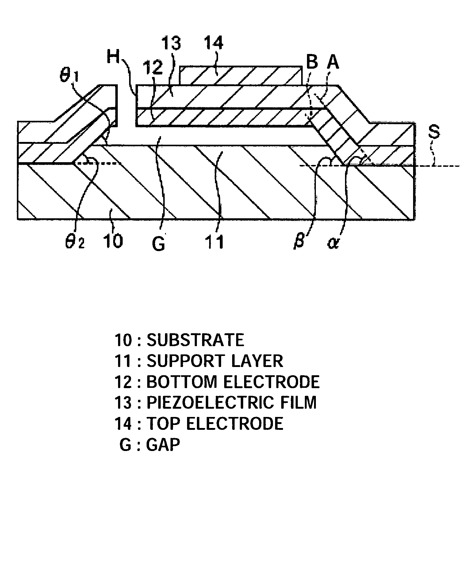
[0120] In a thin film bulk acoustic wave resonator according to an embodiment having composition shown in FIG. 1, it was examined about generation of breakage (crack) and destruction (peeling off) of the piezoelectric film 13 when the height of the support layer 11 formed from a portion of the silicon substrate 10 is changed variously to 0%, 5%, 10%, 15%, 20% and 25% of a height of the sacrificial layer 31 in the gap region between the silicon substrate 10 and the bottom electrode 12.

[0121] As a result, when the height of the support layer 11 is between 0% and 5% of the height of the sacrificial layer 31, generation of a crack of the piezoelectric film 13 was observed. Further, when 10%, generation of destruction of the piezoelectric film 13 was not observed, however, breakage of the piezoelectric film 13 was observed. When it became the height of 15%, generation of breakage was observed occasionally, however, when the height became 20% or more of the piezoelectric film 13 generati...


PUM


Abstract

A thin film bulk acoustic wave resonator and method of producing same are provided. The thin film bulk acoustic wave resonator has a superior resonance characteristic (e.g., highly-orientation and densification of a piezoelectric film), wherein the thin film bulk acoustic wave resonator that a local stress to a piezoelectric film is relaxed and improvement of productivity due to a stable structure causing a crack of the piezoelectric film and high yield and a corresponding cost-reduction are realized, and the production method of the same, such as in an air bridge type thin film bulk acoustic wave resonator. A region including a substrate, a support layer formed convexly on the substrate and a gap upper than the support layer has a laminate of a bottom electrode, a piezoelectric film and an upper layer, where the laminate is formed on the substrate and the support layer. The gap is formed between the support layer and the bottom electrode so that at least a portion of it is located upper than a surface of the support layer, and is composed a resonance region. For example, the support layer has a height of 20% or more of the maximum height from the support layer surface to the top of the gap.

Description

CROSS REFERENCE TO RELATED APPLICATIONS [0001] The present application claims priority to Japanese Patent Document No. P2004-041356 filed on Feb. 18, 2004, the disclosure of which is herein incorporated by reference. BACKGROUND OF THE INVENTION [0002] The present invention relates to a thin film bulk acoustic wave resonator and the production method of the same. [0003] A film bulk acoustic wave resonator (FBAR) excelling in a filter characteristic and making it possible to a miniaturization of the RF front-end module receives an attention as an element used in a circuit such as a transmission filter and a duplexer in a wireless communication system such as a mobile phone and a wireless sensing system. [0004] As a structure and a production method of the above-mentioned FBAR, methods such as (1) a substrate topside-depression method, (2) a substrate backside-via-hole method, (3) an air bridge method, (4) a multilayer acoustic mirror method are known. [0005] In the above, an air bridg...

Claims


Application Information

Patent Timeline
Patent Type & Authority Applications(United States)
IPC IPC(8): H01L41/18H01L41/09H01L41/22H01L41/29H01L41/316H03H3/02H03H9/02H03H9/17H03H9/54
CPCH03H3/02H03H9/172H03H9/02133
Inventor SATO, SUSUMU
Owner SONY CORP
Why Eureka
Try Eureka