Customizable development and demonstration platform for structured ASICs

Active Publication Date: 2005-08-18
BELL SEMICON LLC
View PDF7 Cites 33 Cited by
  • Summary
  • Abstract
  • Description
  • Claims
  • Application Information

AI Technical Summary

Benefits of technology

[0007] Accordingly, the present invention is directed to a customizable development and demonstration platform for structured ASICs. In an exemplary aspect of the present invention, a customizable development and demonstration platform for structured ASICs may include a structured ASIC which is built on a slice and which may be flexible enough for a number of possible application developments. For example, a structured ASIC may be a RapidChip™, and a slice may be a RapidSlice™. This flexibility may be achieved by incorporating a programmable processor in the structured ASIC and by defining interfaces and the use of an external Field Programmable Gate Array (FPGA) in the present platform. The structured ASIC may include a complete ARM processor subsystem and a plurality of high speed SERDES (serializer-deserializer) ports. The processor subsystem may include a bus interface to the external FPGA, allowing custom gate development and test in the FPGA, prior to incorporating it into the customer product. The number of the plurality of high speed SERDES ports 106 may be eight. The eight high speed SERDES ports may be used as follows: 1 port is driven by test circuitry or test block to more readily run signal integrity tes

Problems solved by technology

However, a slice is still fully decoupled because the customer has not yet introduced the function into the slice.
Conventionally, a demonstration and development platform may involve the following methods: (1) software simulation (However, such a method may be custom developed per project and tends to execute very slowly.
Moreover, there is no proof of actual hardware); (2) board based solutions using stand

Method used


Image

  • Customizable development and demonstration platform for structured ASICs
  • Customizable development and demonstration platform for structured ASICs
  • Customizable development and demonstration platform for structured ASICs

Examples


Embodiment Construction

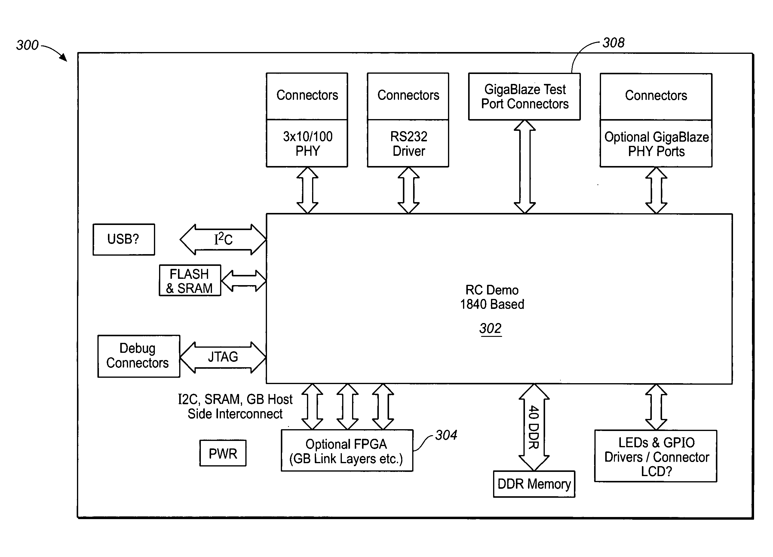
[0014] Reference will now be made in detail to the presently preferred embodiments of the invention, examples of which are illustrated in the accompanying drawings.

[0015] Referring first to FIG. 1, a schematic block diagram illustrating an exemplary RapidChip™100 in accordance with an exemplary embodiment of the present invention is shown. The RapidChip™100 may be part of a customizable development and demonstration platform (e.g., a demo board, and the like) in accordance with the present invention. It is understood that other structured ASICs may be used in the present invention without departing from the scope and spirit of the present invention. The RapidChip™100 may be built on a RapidSlice™102 and may be flexible enough for a number of possible application developments. This flexibility may be achieved by incorporating a programmable processor in the RapidChip™100 and by defining interfaces and the use of an external Field Programmable Gate Array (FPGA) (not shown) in the pre...


PUM


Abstract

The present invention is directed to a customizable development and demonstration platform for structured ASICs. In an exemplary aspect of the present invention, the present platform may include a structured ASIC which is built on a slice and which may be flexible enough for a number of possible application developments. This flexibility may be achieved by incorporating a programmable processor in the structured ASIC and by defining interfaces and the use of an external FPGA in the present platform. The structured ASIC may include a complete ARM processor subsystem and a plurality of high speed SERDES ports. The processor subsystem may include a bus interface to the external FPGA, allowing custom gate development and test in the FPGA, prior to incorporating it into the customer product. Through the SERDES ports, the test block may be used to show the electrical characteristics of the SERDES IP. In addition, some SERDES ports may be driven from a link layer realized in the FPGA. This may allow the same chip and board to implement SATA (serial advanced technology attachment), GigE, XAUI, XGXS, Fibre Channel, and the like by changing the programming of the FPGA on the board.

Description

FIELD OF THE INVENTION [0001] The present invention relates generally to integrated circuits, and particularly to a customizable development and demonstration platform for structured ASICs. BACKGROUND OF THE INVENTION [0002] A structured ASIC (application specific integrated circuit) is a large-scale, high-complexity semiconductor device that includes one or more of the following elements: (1) memory; (2) a customizable array of transistors; (3) an IP (intellectual property) block; (4) a processor, e.g., an ESP (embedded standard product); (5) an embedded programmable logic block; and (6) interconnect. RapidChip™ developed by LSI Logic Corp. is an example of a structured ASIC. [0003] Structured ASIC based IC design is a powerful concept for coping with the increased pressure on time-to-market, design and manufacturing costs. The basic idea behind structured ASIC based IC design is to avoid designing a chip from scratch. Some portion of the chip's architecture is predefined for a spe...

Claims


Application Information

Patent Timeline
IPC IPC(8): G06F17/50
CPCG06F2217/64G06F17/5045G06F30/30G06F2115/06
Inventor VOGEL, DANNYSHAW, CARL
Owner BELL SEMICON LLC
Why Eureka
Try Eureka