Composite microelectronic spring structure and method for making same

a micro-electronic and spring structure technology, applied in the direction of contacts, instruments, and semiconductor/solid-state device details, etc., can solve the problems of not being able becoming increasingly difficult to meet these, and other design requirements, and unable to meet the design requirements described. , to achieve the effect of convenient use, adequate strength and stability, and less time and expens

Inactive Publication Date: 2006-06-20
FORMFACTOR INC
View PDF56 Cites 36 Cited by
  • Summary
  • Abstract
  • Description
  • Claims
  • Application Information

AI Technical Summary

Benefits of technology

[0011]The other of the parent applications, Ser. No. 09 / 023,859 referenced above, describes a composite column element comprised of post, beam, and tip components, each of which are fabricated lithographically by depositing layers of metallic materials in patterns on various sacrificial substrates. The post, beam, and tip components are then assembled into a contact structure. In particular, the post component is formed by depositing a relatively thick layer of metallic or other conductive material in a recess formed in a relatively thick layer of photo-resist. The present invention eliminates the need to deposit these relatively thick layers.
[0013]The present invention thus provides at least the following advantages over the structures disclosed in the foregoing parent applications. The plural, ball-bonded columns require much less time and expense to manufacture compared to the lithographically fabricated column elements formed by deposition of a material on a substrate. This is particularly true when column elements that extend from the electronic substrate for more than about 50 microns (about 2 mils) are desired, because deep layering of photoresist materialsis avoided. Ball-bonded columns also eliminate the need for relatively time-consuming plating processes or other deposition of post materials. Additionally, grouped, plural columns as contemplated in an embodiment of the present invention may be made relatively long and slender while retaining adequate strength and stability. Such long, slender columns provide adjustability for the position of the spring contact tips. For example, contact tips that are manufactured slightly out of position may be restored to a correct position by slightly bending (i.e., plastically deforming) each column in an appropriate way, while the group of columns as a whole remains relatively rigid and stable. Plural columns are also more versatile than single post components, and are amenable for use in a wider variety of designs. The plural columns of the present invention also provide benefits for the electrical performance of a spring contact, such as reduced capacitance.

Problems solved by technology

However, such techniques are not well suited for meeting the design requirements described below.
Such terminals are often contaminated with organic films, corrosion, or oxides on their contact surfaces, and the tip of the spring contact must be applied with sufficient force to penetrate this barrier of contamination.
When spring contacts are fabricated at ever-smaller microelectronic scales, it becomes increasingly difficult to fulfill these, and other, design requirements.

Method used


Image

  • Composite microelectronic spring structure and method for making same
  • Composite microelectronic spring structure and method for making same
  • Composite microelectronic spring structure and method for making same

Examples


Embodiment Construction

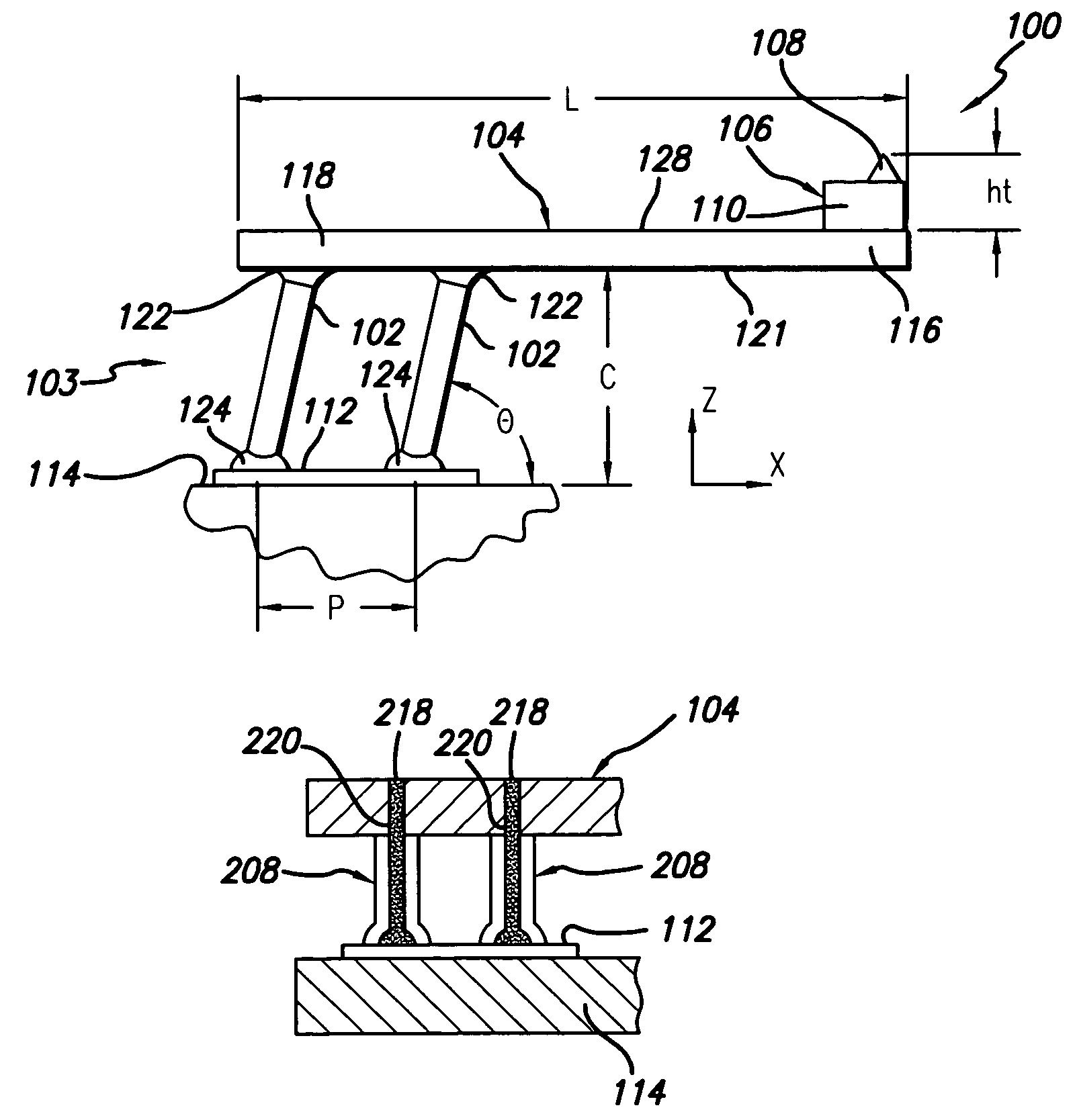
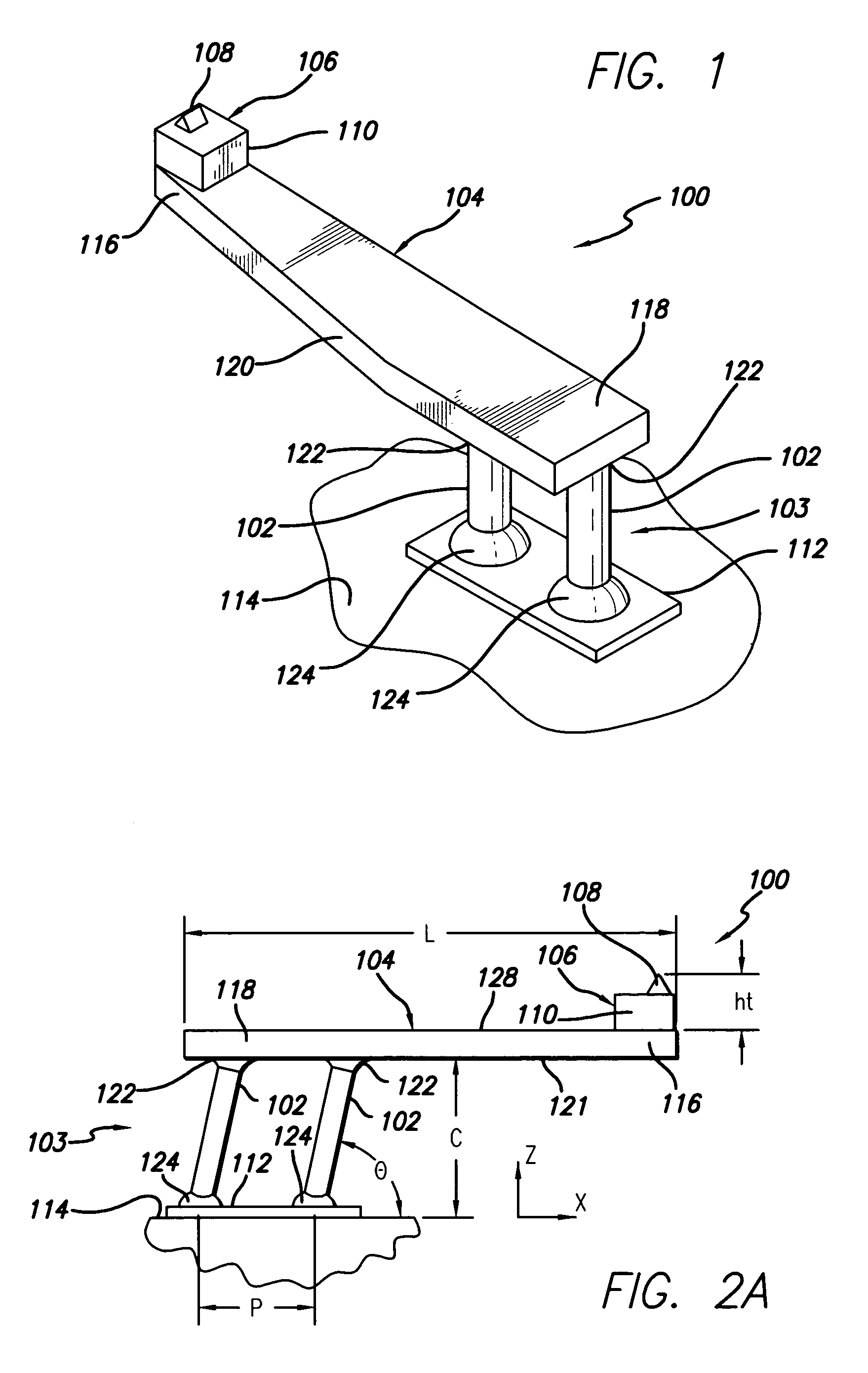
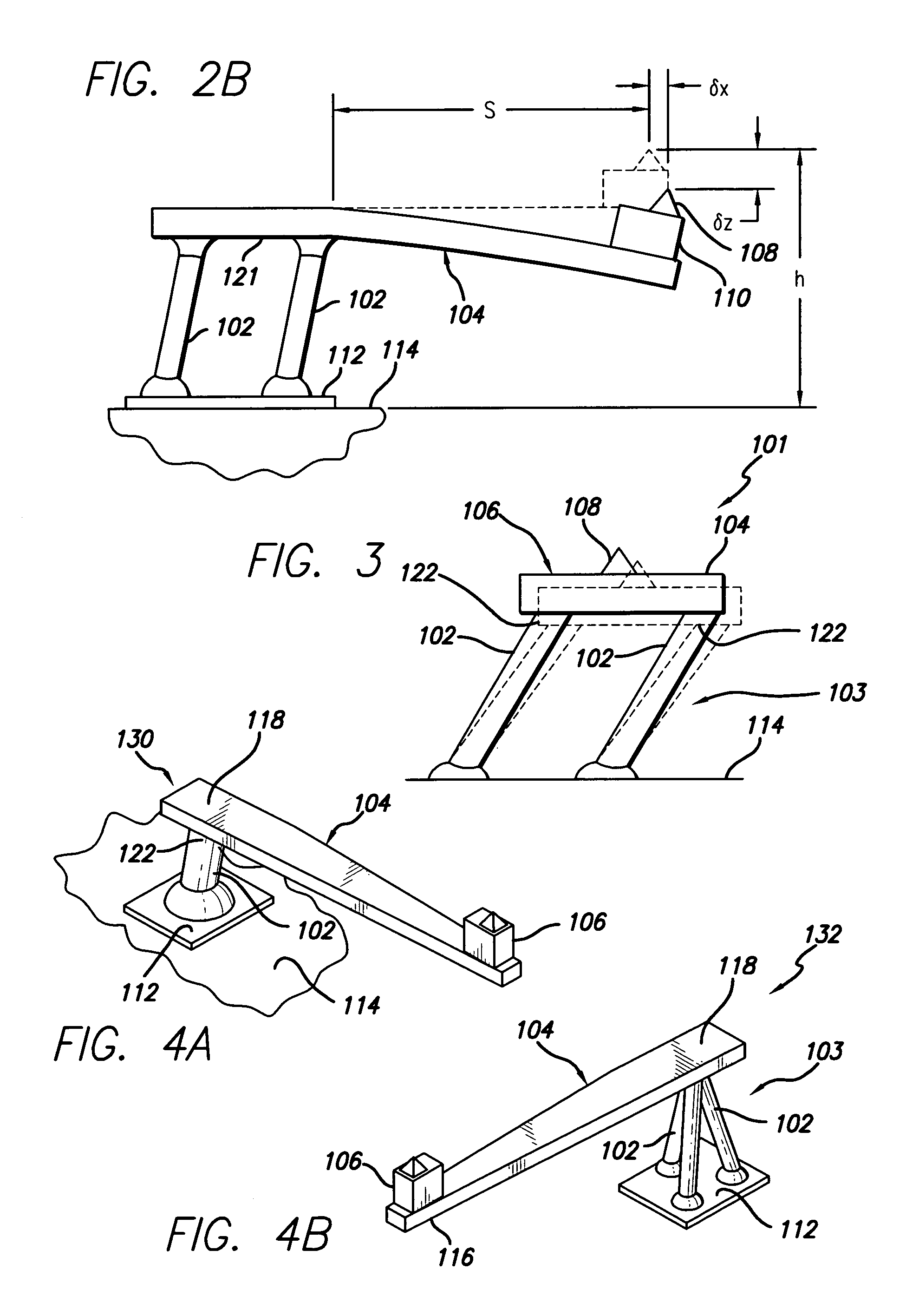
[0042]The present invention satisfies the need for a microelectronic spring structure, that overcomes the limitations of prior art spring structures. In the detailed description that follows, like element numerals are used to describe like elements illustrated in one or more figures.

[0043]Contact structures according to the present invention are particularly well-suited to making electrical connections to microelectronic devices having contact pads disposed at a fine-pitch, or where a large array of economical microelectronic spring contacts is desired; and particularly where a relatively large z-extension, such as greater than about 130 microns (5 mils), is desired. As used herein, the term “fine-pitch” refers to microelectronic devices that have their contact pads disposed at a spacing of less than about 130 microns (5 mils), such as 65 microns (2.5 mils). However, structures of the present invention may also be used in coarser-pitch applications, if desired. The advantages of the...


PUM


Abstract

An improved microelectronic spring structure, and method of making the same, are disclosed. The improvement comprises, in a spring contact of the type comprising a beam attached to a post, of replacing the post with a plurality of column elements. The beam component is thus provided with one or more column elements which both structurally support and electrically connect one end of the beam to an electronic component. The column elements are preferably comprised of relatively straight segments of wire elements that are ball-bonded to a substrate and are over-coated with suitable structural and / or conducting materials. In the alternative, the improvement comprises a single column element comprised of a relatively straight segment of wire that is ball-bonded to a substrate and over-coated with suitable structural and conducting materials, wherein the column element is essentially rigid. The improved spring structures are especially useful for use as spring contacts on substrates such as probe cards, interposers, semiconductor devices, and other electronic components.

Description

RELATED APPLICATION[0001]This application is a continuation-in-part of commonly-owned, application Ser. No. 09 / 023,859, filed Feb. 13, 1998 (now U.S. Pat. No. 6,520,778), and commonly-owned, application Ser. No. 08 / 819,464, filed Mar. 17, 1997, both of which are incorporated, in their entirety, by reference herein.BACKGROUND OF THE INVENTION[0002]1. Field of the Invention[0003]The present invention relates to electrical interconnection (contact) elements and, more particularly, to contact elements which are resilient contact elements suitable for effecting readily demountable pressure connections between substrates, such as electronic components.[0004]2. Description of Related Art[0005]Readily demountable interconnections between electronic components include resilient spring elements of one electronic component being received by another electronic component at, for example, non-resilient contact elements such as pads or sockets. The spring elements exert a contact force (optionally...

Claims


Application Information

Patent Timeline
Patent Type & Authority Patents(United States)
IPC IPC(8): H01R12/00B81B3/00G01R1/067G01R1/073G01R3/00G01R31/28H01H1/00H01L23/48H01L23/485H01L23/498H05K3/20H05K3/34
CPCG01R1/06727G01R1/07342H01L23/49811H01L24/06H01L24/10H01L24/72G01R1/06744H01L2924/01047H01L2924/01045H01L2924/01033G01R3/00H01H1/0036H01L2224/0401H01L2224/04042H01L2224/06136H01L2924/01004H01L2924/01006H01L2924/01012H01L2924/01013H01L2924/01014H01L2924/01015H01L2924/01022H01L2924/01027H01L2924/01029H01L2924/01039H01L2924/01042H01L2924/01046H01L2924/01049H01L2924/0105H01L2924/01051H01L2924/01074H01L2924/01078H01L2924/01079H01L2924/01082H01L2924/01322H01L2924/014H01L2924/14H01L2924/19041H01L2924/30105H05K3/20H05K3/3421H01L2924/00013H01L2924/01005H01L2924/01019H01L2224/13099H01L2224/29099H01L2924/15787H01L2224/45144H01L2924/00
Inventor GRUBE, GARY W.KHANDROS, IGOR Y.MATHIEU, GAETAN L.
Owner FORMFACTOR INC
Why Eureka
Try Eureka