Plasma antenna

a technology of plasma and antenna, applied in the field of plasma antenna, can solve the problems of difficult control of the distribution of inductive electric field, damage to the insulating plate equipped between the antenna and the vacuum chamber, and damage to the insulating plate, etc., and achieve the effect of maximizing the efficiency of a process

Active Publication Date: 2005-08-25
JUSUNG ENG
View PDF11 Cites 21 Cited by
  • Summary
  • Abstract
  • Description
  • Claims
  • Application Information

AI Technical Summary

Benefits of technology

[0015] The present invention has been made to solve the above problems, and it is an object of the present invention to provide a plasma antenna, designed to allow connection between electric elements of the antenna to be changed, if necessary, to generate series connection type plasma, parallel connection type plasma or capacitive coupled plasma without changing the construction of the antenna in a plasma processing apparatus, thereby maximizing efficiency of a process, such as cleaning and depositing.

Problems solved by technology

However, since the constant electrical current flows through the respective coils, it is difficult to control distribution of an inductive electric field.
As a result, the insulating plate equipped between the antenna and the vacuum chamber can be damaged due to the plasma.
In this case, when the antenna is employed under a higher vacuum level of several mTorr, it generates plasma exhibiting desirable characteristics, whereas when the antenna is employed under a lower vacuum level of several Torr, it often generates partially concentrated plasma, thereby partially damaging the object to be processed.
The primary cause of this is a constructional problem causing the RF power to be concentrated on a specific coil.

Method used


Image

  • Plasma antenna
  • Plasma antenna
  • Plasma antenna

Examples


Embodiment Construction

[0027] Preferred embodiments will now be described in detail with reference to the accompanying drawings.

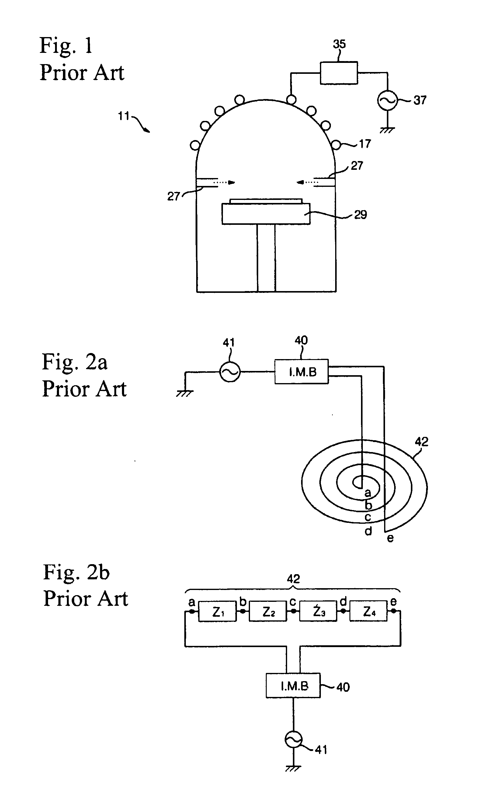
[0028] The present invention may be applied to a high density plasma apparatus, a plasma enhanced chemical vapor deposition (PECVD) apparatus, or a plasma processing apparatus, such as an apparatus for etching. In the following embodiment, a high density plasma processing apparatus of the present invention will be described in detail.

[0029] Conditions for generating the plasma are significantly different in a deposition process and an etching process using plasma. When generating high density plasma by use of an identical inductive coupled plasma apparatus, a plasma processing apparatus for realizing both conditions appropriate for the deposition process and for the etching process is difficult to be implemented.

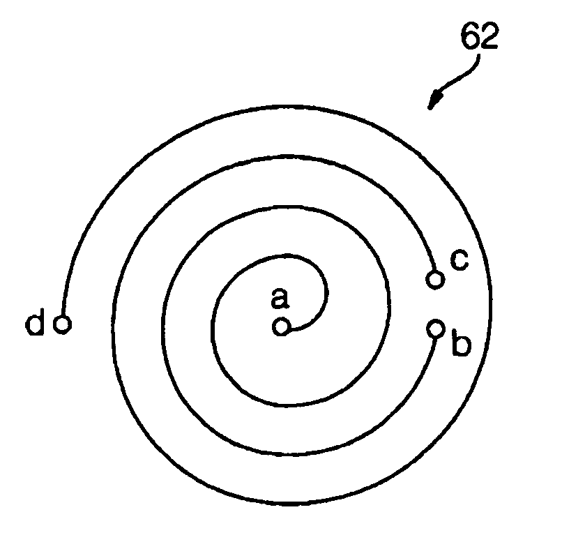
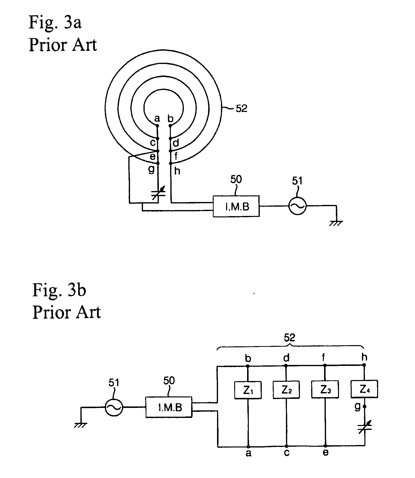
[0030] In the case of an antenna constituting a parallel circuit in which electric elements are connected in parallel, since it has low impedance, high current flows i...


PUM

PropertyMeasurementUnit
impedanceaaaaaaaaaa
helical shapeaaaaaaaaaa
temperatureaaaaaaaaaa

Abstract

The plasma antenna is designed to allow connection between electric elements within the antenna to be varied without changing the construction of the antenna during a chemical vapor deposition process, thereby maximizing efficiency of a cleaning or deposition process. The plasma antenna comprises two or more coils to which RF power is supplied from an RF power source, respectively, and a switch connected to ends of the coils. The coils are constructed to have different impedances. The circuit construction of the plasma antenna can be changed on the basis of an inductive coupled plasma antenna so as to generate parallel connection type plasma, series connection type plasma, or capacitive coupled plasma according to the kind of process, such as cleaning or depositing, without changing the construction of the antenna, so that the process can be performed efficiently, thereby enhancing productivity through reduction in manufacturing costs attributed to the simple construction of the antenna.

Description

BACKGROUND OF THE INVENTION [0001] 1. Field of the Invention [0002] The present invention relates to a plasma antenna for a plasma processing apparatus, and, more particularly, to a plasma antenna, designed to allow connection between electric elements of the antenna to be varied without changing the construction of the antenna during a chemical vapor deposition process, thereby maximizing efficiency of a cleaning or deposition process. [0003] 2. Description of the Prior Art [0004] In manufacture of semiconductor devices, various plasma deposition and etching have been developed. This is attributed to the fact that, in comparison to a commonly used chemical vapor deposition process, the plasma deposition process can be performed at a lower deposition temperature and a higher deposition speed due to activation of reactant gases by the plasma. Additionally, the plasma deposition or etching process can be performed more easily by appropriately applying a relative bias to a plasma elect...

Claims


Application Information

Patent Timeline
Patent Type & Authority Applications(United States)
IPC IPC(8): C23C16/00H01L21/3065C23C16/513H01J37/32H05H1/46
CPCH01J37/321H01L21/3065
Inventor LEE, YONG HYUN
Owner JUSUNG ENG
Why Eureka
Try Eureka