

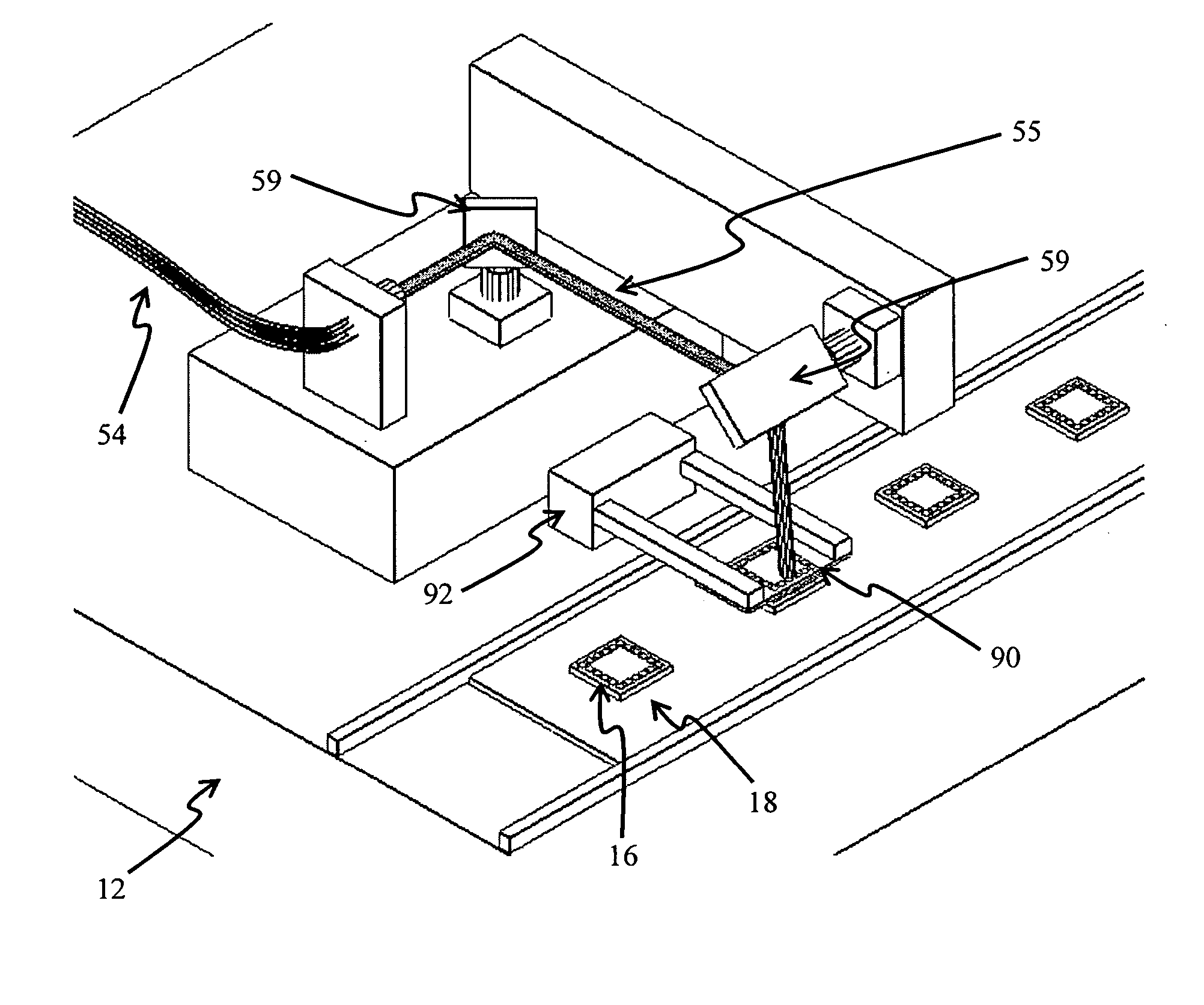
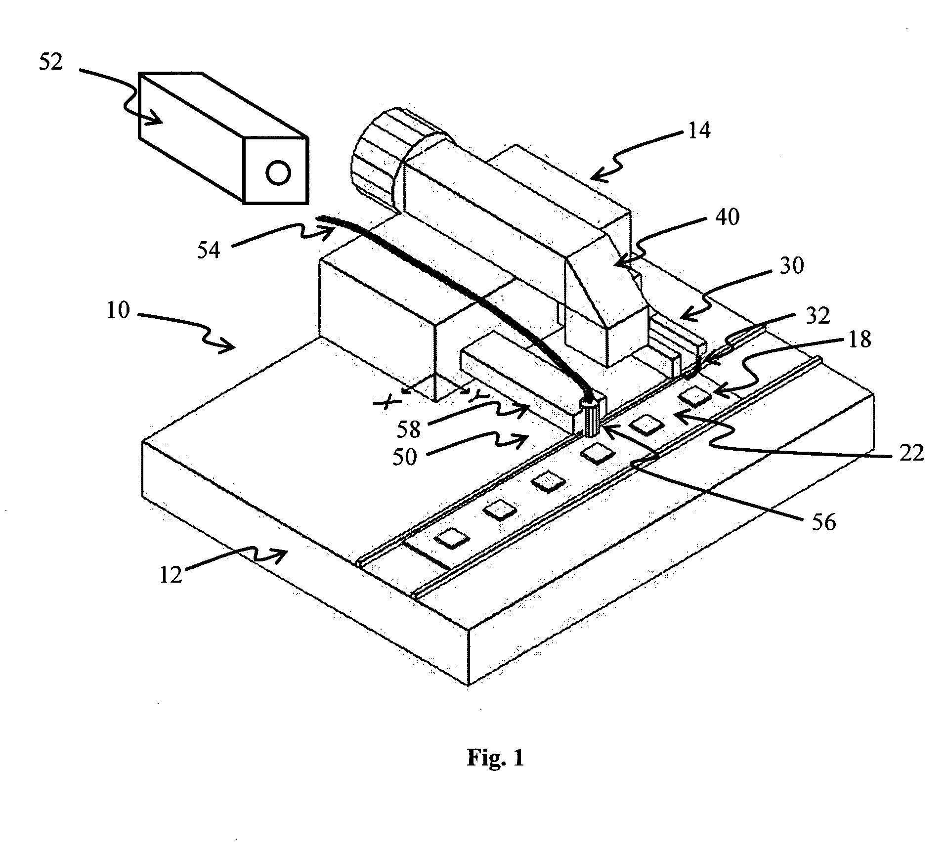
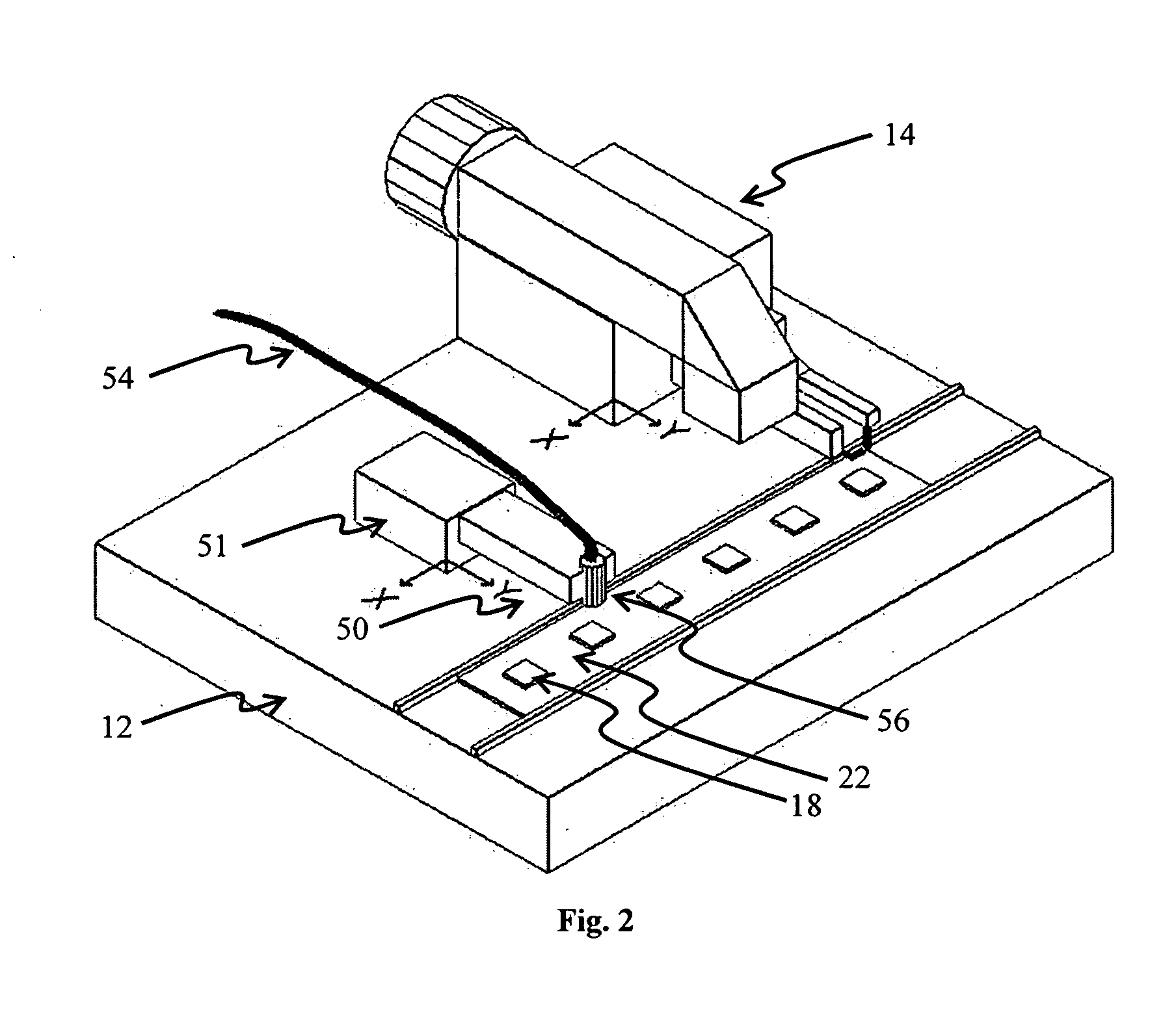
Laser cleaning system for a wire bonding machine
a cleaning system and wire bonding machine technology, applied in the direction of non-electric welding apparatus, welding apparatus, manufacturing tools, etc., can solve the problems of hard aluminum oxides, oxide layers can interfere with the bonding process, adverse effects,
- Summary
- Abstract
- Description
- Claims
- Application Information
AI Technical Summary
Benefits of technology
Problems solved by technology
Method used
Image

Examples
example
[0040] The following example illustrates the effectiveness of laser cleaning for improving the second bond strength of wire-bonded devices. Three test devices were wire bonded on a Kulicke & Soffa model 8028 PPS wire bonder using 1 mil Kulicke & Soffa AW99 gold wire. The test devices were attached to identical plastic ball grid area (BGA) substrates with gold-plated bond pads. Test device A was wire bonded without any cleaning, whereas the gold-plated 2nd bond pads on the substrates for devices B and C were laser-cleaned using a New Wave Research QuickkLaze II Nd-YAG laser prior to wire bonding. Laser cleaning was performed using 532 nm laser light passing through a 20× objective to produce a spot size of approximately 100 μm. The areas to be cleaned on the substrate were passed under the laser beam at a rate of 200 μm / s. The laser was operated at a pulse repetition rate of 40 Hz. The laser power was set to 40% (4 mW) and 50% (5 mW) for cleaning devices B and C, respectively. The st...
PUM
| Property | Measurement | Unit |
|---|---|---|
| wavelength | aaaaa | aaaaa |
| wavelength | aaaaa | aaaaa |
| wavelength | aaaaa | aaaaa |
Abstract
Description
Claims
Application Information