Ultra-thin SOI vertical bipolar transistors with an inversion collector on thin-buried oxide (BOX) for low substrate-bias operation and methods thereof

a vertical bipolar transistor, thin-buried oxide technology, applied in the direction of transistors, semiconductor devices, electrical equipment, etc., can solve the problems of unsatisfactory high bias, achieve high bias, reduce manufacturing costs, simplify the integration scheme

Active Publication Date: 2005-08-25
GLOBALFOUNDRIES US INC
View PDF6 Cites 23 Cited by
  • Summary
  • Abstract
  • Description
  • Claims
  • Application Information

AI Technical Summary

Benefits of technology

[0007] The present invention overcomes the problems of prior art vertical SOI BJTs by providing a “collector-less” SOI BJT which has no impurity-doped collector. Instead, the inventive vertical SOI BJT uses a back gate-induced, minority carrier inversion layer as the intrinsic collector when it operates. In accordance with the present invention, the SOI substrate is biased such that an inversion layer is formed at the bottom of the base region serving as the collector. The advantage of such a device is its CMOS-like process. Therefore, the integration scheme can be simplified and the manufacturing cost can be significantly reduced. However, for a typical SOI substrate with a buried oxide (BOX) thickness of 100 nm, a substrate bias of 30 V is required in order to generate the inversion layer. Such a high bias is not desirable. In order for such a bipolar device to be practical for BiCMOS on SOI applications, the substrate bias should be equal to or less than the bias applied to the CMOS, typically 3 V or less.
[0008] The present invention also provides a method of fabricating BJTs on areas of a very thin BOX using a conventional SOI starting wafer with a thick BOX. The reduced BOX thickness underneath the bipolar devices allows for a significantly reduced substrate bias compatible with the CMOS to be applied while maintaining the advantages of a thick BOX underneath the CMOS.
[0011] The device structure of the present invention can provide complementary BJTs and can be integrated directly with the current SOI CMOS technology. Hence, a complementary Bi / CMOS can be realized and provide new opportunities for circuit innovations. In one embodiment, a field effect transistor is formed in areas adjacent to the bipolar transistor of the present invention, said transistors being separated by trench isolation regions.

Problems solved by technology

Such a high bias is not desirable.

Method used


Image

  • Ultra-thin SOI vertical bipolar transistors with an inversion collector on thin-buried oxide (BOX) for low substrate-bias operation and methods thereof
  • Ultra-thin SOI vertical bipolar transistors with an inversion collector on thin-buried oxide (BOX) for low substrate-bias operation and methods thereof
  • Ultra-thin SOI vertical bipolar transistors with an inversion collector on thin-buried oxide (BOX) for low substrate-bias operation and methods thereof

Examples


Embodiment Construction

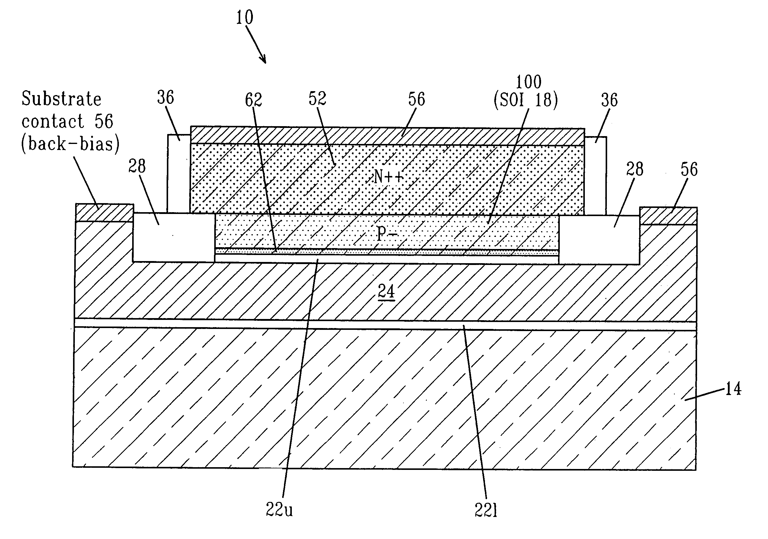
[0030] The present invention, which provides an ultra-thin SOI vertical bipolar transistor with an inversion collector on a thin BOX for low substrate bias operation and a method of fabricating the same, will now be described in more detail by referring to the drawings that accompany the present application.

[0031] As stated above, the present invention provides a bipolar transistor structure that includes a conductive back electrode for receiving a bias voltage, an insulating layer located over the conductive back electrode, and a first semiconductor layer located over the insulating layer. The first semiconductor layer includes a base containing a first conductive type dopant and an extrinsic collector containing a second conductivity type dopant. In accordance with the present invention, the extrinsic collector borders the base. The inventive bipolar transistor also includes an emitter comprising a second semiconductor layer of the second conductivity type dopant located over a p...


PUM


Abstract

The present invention provides a “collector-less” silicon-on-insulator (SOI) bipolar junction transistor (BJT) that has no impurity-doped collector. Instead, the inventive vertical SOI BJT uses a back gate-induced, minority carrier inversion layer as the intrinsic collector when it operates. In accordance with the present invention, the SOI substrate is biased such that an inversion layer is formed at the bottom of the base region serving as the collector. The advantage of such a device is its CMOS-like process. Therefore, the integration scheme can be simplified and the manufacturing cost can be significantly reduced. The present invention also provides a method of fabricating BJTs on selected areas of a very thin BOX using a conventional SOI starting wafer with a thick BOX. The reduced BOX thickness underneath the bipolar devices allows for a significantly reduced substrate bias compatible with the CMOS to be applied while maintaining the advantages of a thick BOX underneath the CMOS.

Description

FIELD OF THE INVENTION [0001] The present invention relates to semiconductor devices, and more particularly to a vertical bipolar transistor that does not include an impurity-doped collector. Instead, the bipolar transistor of the present invention contains a minority carrier inversion layer as the collector. The present invention also provides a method for forming such a vertical bipolar transistor. BACKGROUND OF THE INVENTION [0002] The semiconductor industry has been seeking more cost effective solutions for manufacturing integrated bipolar transistors and complementary metal oxide semiconductor (CMOS) devices (hereinafter Bi / CMOS) for mass applications of radio frequency (RF) / analog and wireless / fiber-based telecommunications for decades. Si / SiGe BiCMOS technology is widely used and has been quite successful. However, as CMOS adopts the thin silicon-on-insulator (SOI) substrate for lower power and higher speed (due to device scaling), the thick sub-collector of conventional bipo...

Claims


Application Information

Patent Timeline
Patent Type & Authority Applications(United States)
IPC IPC(8): H01L21/331H01L21/8222H01L21/8248H01L21/8249H01L27/06H01L27/08H01L27/082H01L27/12H01L29/73H01L29/732
CPCH01L29/7317
Inventor HO, HERBERT L.KUMAR, MAHENDEROUYANG, QIQINGPAPWORTH, PAUL A.SHERAW, CHRISTOPHER D.STEIGERWALT, MICHAEL D.
Owner GLOBALFOUNDRIES US INC
Why Eureka
Try Eureka