Spin transfer magnetic element having low saturation magnetization free layers

a magnetic element and free layer technology, applied in the field of magnetic memory systems, can solve the problems of large transistor size and high power consumption, and achieve the effect of low saturation magnetization and low saturation magnetization

Active Publication Date: 2005-08-25
SAMSUNG SEMICON
View PDF6 Cites 242 Cited by
  • Summary
  • Abstract
  • Description
  • Claims
  • Application Information

AI Technical Summary

Benefits of technology

[0011] According to the system and method disclosed herein, the present invention provides a magnetic element that can be switched due to spin transfer using a lower current density.

Problems solved by technology

The high operating current leads to design problems for high density MRAM, such as heating, high power consumption, large transistor size, as well as other issues.

Method used


Image

  • Spin transfer magnetic element having low saturation magnetization free layers
  • Spin transfer magnetic element having low saturation magnetization free layers
  • Spin transfer magnetic element having low saturation magnetization free layers

Examples


first embodiment

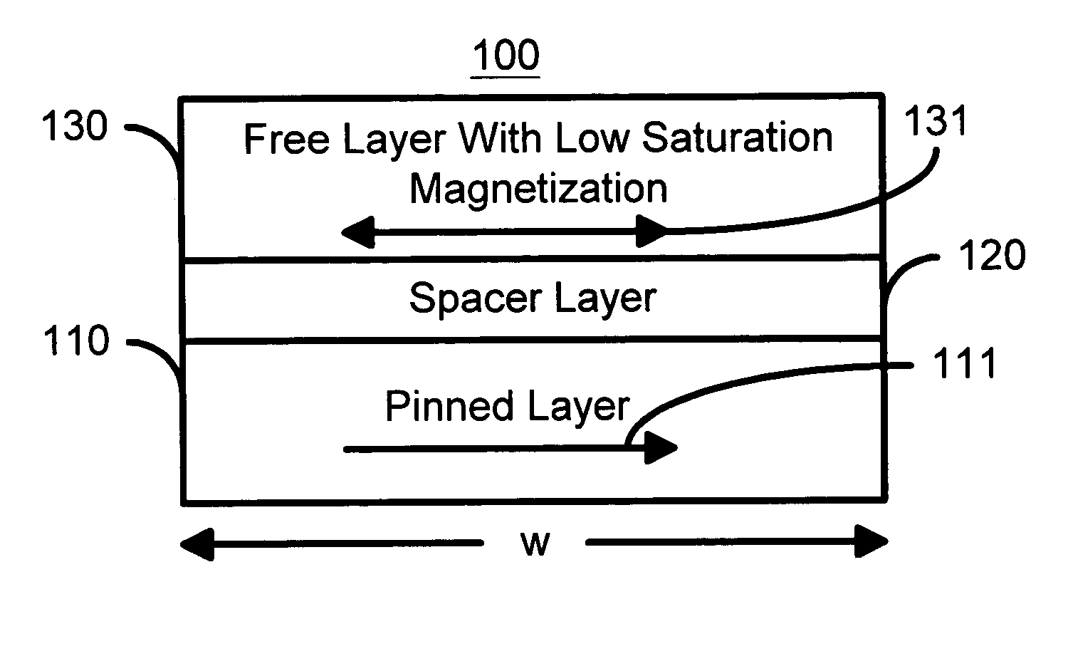
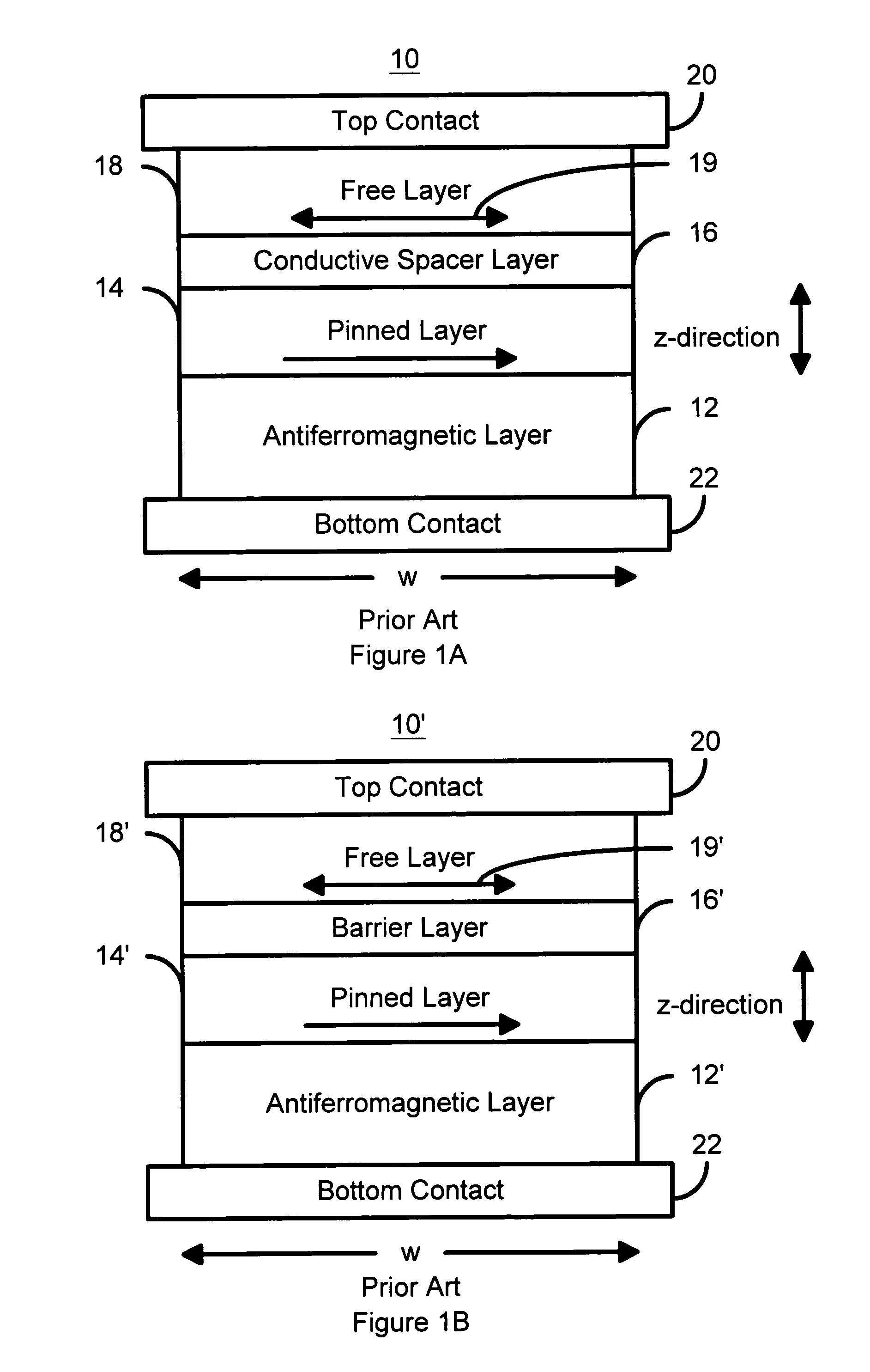
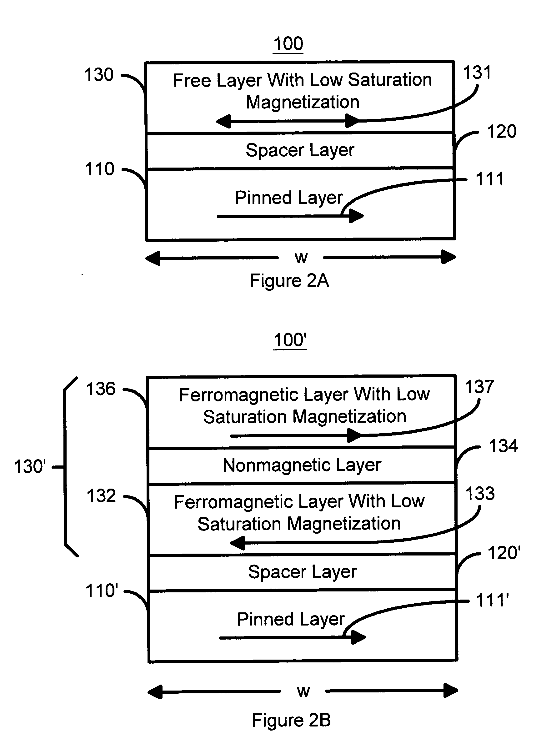
[0027] To more particularly illustrate the method and system in accordance with the present invention, refer now to FIG. 2A, depicting a portion of a magnetic element 100 in accordance with the present invention having a reduced write current density for spin transfer. The magnetic element 100 is preferably used in a magnetic memory, such as a MRAM. Thus, the magnetic element 100 may be used in a memory cell including an isolation transistor (not shown), as well as other configurations of magnetic memories. Moreover, the magnetic element 100 preferably utilizes two terminals (not shown) near the top and bottom of the magnetic element. However, nothing prevents the use of another number of terminals, for example a third terminal near the center of the magnetic element. The magnetic element 100 includes a pinned layer 110, a spacer layer 120, and a free layer 130. As described below, the free layer 130 is configured to have a low saturation magnetization. The magnetic element 100 gene...

second embodiment

[0045]FIG. 4 depicts a magnetic element 200 in accordance with the present invention having a reduced write current density for spin transfer. The magnetic element 200 includes a spin valve portion 204 and a spin tunneling junction portion 202 that share a free layer 230. The spin valve portion 204 includes a pinning layer 260 that is preferably an antiferromagnetic (AFM) layer 260, pinned layer 250, conductive spacer layer 240 such as Cu, and a free layer 230. In an alternate embodiment, the conductive spacer layer 240 could be replaced by a barrier layer. The spin tunneling junction portion 202 includes a pinning layer 206 that is preferably an antiferromagnetic (AFM) layer 206, pinned layer 210, barrier layer 220 that is an insulator configured to allow electrons to tunnel through it, and the free layer 230. Referring to FIGS. 2A and 4, the layers 250, 240, and 230 are analogous to the layers 110, 120, and 130 in the magnetic element 100 when the spacer layer 120 is conducting. S...

third embodiment

[0051]FIG. 6 depicts a portion of a magnetic element 400 in accordance with the present invention having a reduced write current density for spin transfer. The magnetic element includes two structures 402 and 404, each of which is analogous to the magnetic element 100, 100′, or 100″. Thus, the structure 402 includes a pinned layer 410, a spacer layer 420, and a free layer 430 that are analogous to, for example, the layers 110, 120, and 130, respectively, of the magnetic element 100. The structure 402 also includes pinning layer 406 that is preferably an AFM layer. Similarly, the structure 404 includes a pinned layer 470, a spacer layer 460, and a free layer 450 that are analogous to, for example, the layers 110, 120, and 130, respectively, of the magnetic element 100. The structure 404 also includes pinning layer 480 that is preferably an AFM layer. One or both of the free layers 430 and 450 have a low saturation magnetization. The free layer 430 and / or 450 may also be synthetic. In...


PUM

PropertyMeasurementUnit
thicknessaaaaaaaaaa
thicknessaaaaaaaaaa
resistanceaaaaaaaaaa

Abstract

A method and system for providing a magnetic element that can be used in a magnetic memory is disclosed. The magnetic element includes pinned, nonmagnetic spacer, and free layers. The spacer layer resides between the pinned and free layers. The free layer can be switched using spin transfer when a write current is passed through the magnetic element. The magnetic element may also include a barrier layer, a second pinned layer. Alternatively, second pinned and second spacer layers and a second free layer magnetostatically coupled to the free layer are included. In one aspect, the free layer(s) include ferromagnetic material(s) diluted with nonmagnetic material(s) and / or ferrimagnetically doped to provide low saturation magnetization(s).

Description

FIELD OF THE INVENTION [0001] The present invention relates to magnetic memory systems, and more particularly to a method and system for providing a magnetic element that employs a spin transfer effect in switching, and that can be switched using a lower switching current density. BACKGROUND OF THE INVENTION [0002]FIGS. 1A and 1B depict conventional magnetic elements 10 and 10′. The conventional magnetic element 10 is a spin valve and includes a conventional antiferromagnetic (AFM) layer 12, a conventional pinned layer 14, a conventional conductive spacer layer 16 and a conventional free layer 18. Other layers (not shown), such as seed or capping layer may also be used. The conventional pinned layer 14 and the conventional free layer 18 are ferromagnetic. Thus, the conventional free layer 18 is depicted as having a changeable magnetization 19. The conventional conductive spacer layer 16 is nonmagnetic. The AFM layer 12 is used to fix, or pin, the magnetization of the pinned layer 14...

Claims


Application Information

Patent Timeline
Patent Type & Authority Applications(United States)
IPC IPC(8): G11C11/15G11C11/16H01F10/16H01F10/32H01F41/30H01H9/00H01L43/10
CPCB82Y25/00B82Y40/00G11C11/16H01L43/10H01F10/3263H01F10/3272H01F41/303H01F10/16G11C11/161H10N50/85
Inventor NGUYEN, PAUL P.HUAI, YIMINGDIAO, ZHITAOALBERT, FRANK
Owner SAMSUNG SEMICON
Why Eureka
Try Eureka