Formation of CIGS absorber layer materials using atomic layer deposition and high throughput surface treatment

a technology of absorber layer and cigs, which is applied in the direction of sustainable manufacturing/processing, final product manufacturing, coatings, etc., can solve the problems of high level of ga in the middle of the cigs absorber layer negatively affecting device function, challenges and disadvantages, and the inability to control the stoichiometric ratio and achieve high volume production with prior art techniques

Inactive Publication Date: 2005-08-25
AERIS CAPITAL SUSTAINABLE IP
View PDF16 Cites 165 Cited by
  • Summary
  • Abstract
  • Description
  • Claims
  • Application Information

AI Technical Summary

Problems solved by technology

A central challenge in constructing a highly efficiency CIGS-based solar cell is that the elemental components of the CIGS layer must be present in a fairly narrow stoichiometric ratio relative to one another in order for the resulting cell to be highly efficient.
It is difficult to control the stoichiometric ratios and achieve high volume production with prior art techniques.
Second, a relatively high level of Ga in the middle of the CIGS absorber layer negatively impacts device function, as small CuGaSe grains form.
Unfortunately, there are several challenges and disadvantages associated with evaporation as a deposition technique for the CIGS absorber layer.
For example, it is difficult to deposit many compounds and alloy compositions by evaporation.
Evaporation deposition is limited to line-of-sight and limited-area sources, which tends to result in poor surface coverage and spatial non-uniformity.
Line-of-sight trajectories and limited-area sources can also result in poor film-thickness uniformity over large areas.
In addition, evaporation deposition techniques typically have relatively few processing parameters that can be varied to tune the properties of the resulting film.
Furthermore, the intermixing of the elements from evaporative sources occurs not only atomically but also as the interaction of discrete atomic clusters, resulting in locally non-uniform deposition in all three dimensions.
Such non-uniformity also alters the local stoichiometric ratios of the absorber layer, decreasing the potential power conversion efficiency of the complete device.
Further, the use of evaporation can result in uneven surfaces that can further degrade the device performance.
It is extremely difficult, if not impossible to reproducibly control the gradation of the individual components of the absorber layer at the atomic or sub-monolayer level.
Finally, the creation of a bandgap graded absorber layer using evaporative sources requires a relatively expensive real-time monitoring system to assess the relative composition of the absorber layer as it is being construct...

Method used


Image

  • Formation of CIGS absorber layer materials using atomic layer deposition and high throughput surface treatment
  • Formation of CIGS absorber layer materials using atomic layer deposition and high throughput surface treatment
  • Formation of CIGS absorber layer materials using atomic layer deposition and high throughput surface treatment

Examples


Embodiment Construction

[0023] Although the following detailed description contains many specific details for the purposes of illustration, anyone of ordinary skill in the art will appreciate that many variations and alterations to the following details are within the scope of the invention. Accordingly, the exemplary embodiments of the invention described below are set forth without any loss of generality to, and without imposing limitations upon, the claimed invention.

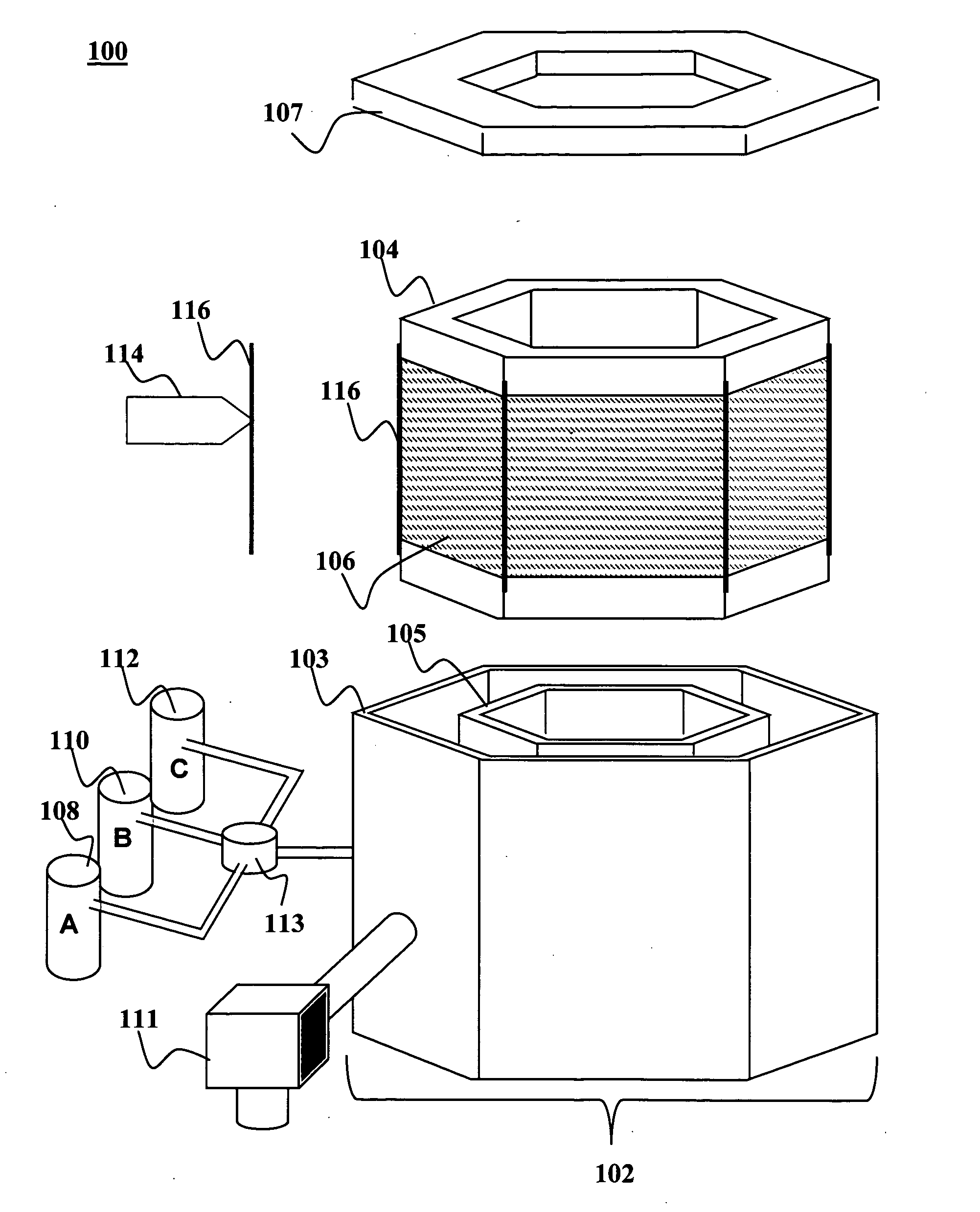
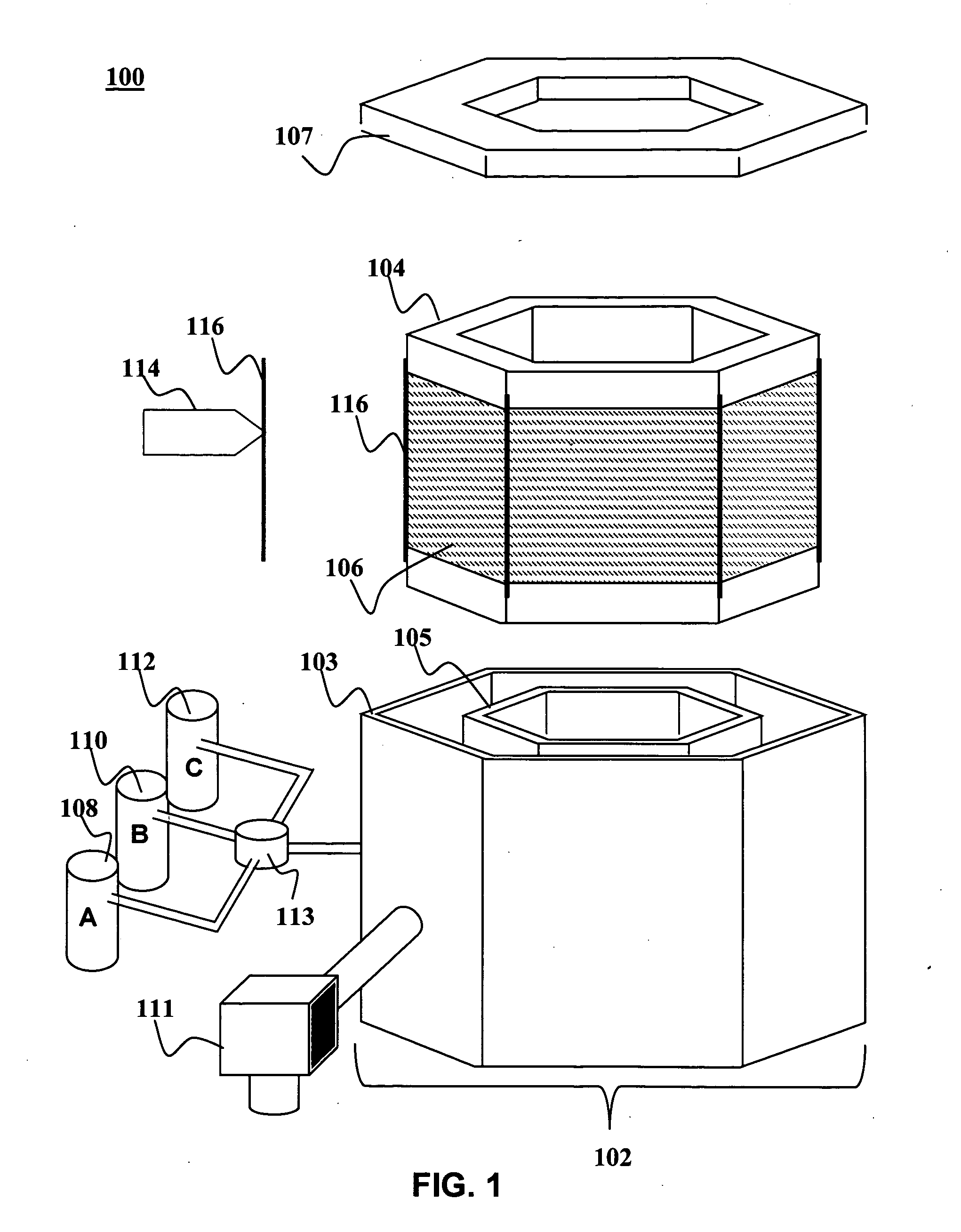
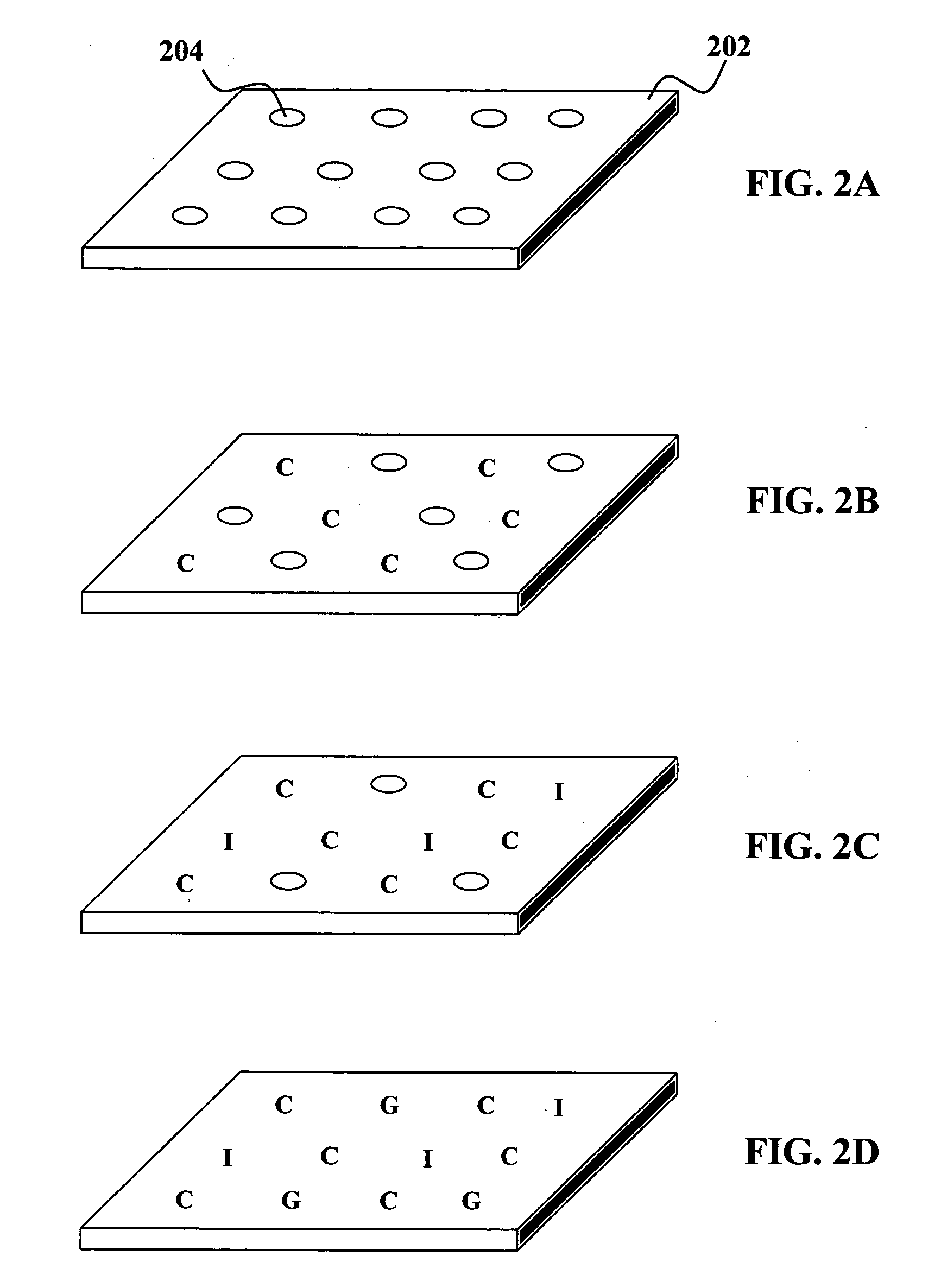
[0024] According to embodiments of the present invention, an absorber layer may be formed on a substrate using atomic layer deposition reactions. An absorber layer containing elements of groups IB, IIIA and VIB may be formed by placing a substrate in a treatment chamber and performing atomic layer deposition of a a group IB element and / or one or more group IIIA elements from separate sources onto a substrate to form a film. A group VIA element is then incorporated into the film and annealed to form the absorber layer. The absorber layer ma...


PUM

PropertyMeasurementUnit
Temperatureaaaaaaaaaa
Thicknessaaaaaaaaaa

Abstract

An absorber layer may be formed on on a substrate using atomic layer deposition reactions. An absorber layer containing elements of groups IB, IIIA and VIB may be formed by placing a substrate in a treatment chamber and performing atomic layer deposition of a group IB element and/or one or more group IIIA elements from separate sources onto a substrate to form a film. A group VIA element is then incorporated into the film and annealed to form the absorber layer. The absorber layer may be greater than about 25 nm thick. The substrate may be coiled into one or more coils in such a way that adjacent turns of the coils do not touch one another. The coiled substrate may be placed in a treatment chamber where substantially an entire surface of the one or more coiled substrates may be treated by an atomic layer deposition process. One or more group IB elements and/or one or more group IIIA elements may be deposited onto the substrate in a stoichiometrically controlled ratio by atomic layer deposition using one or more self limiting reactions.

Description

CROSS-REFERENCE TO RELATED APPLICATION [0001] This application is a continuation-in-part of commonly-assigned co-pending U.S. patent application Ser. No. 10 / 782,545, which was filed Feb. 19, 2004, the entire disclosures of which are incorporated herein by reference. This application is also related to commonly-assigned, co-pending application Ser. No. 10 / 782,233, titled “ROLL-TO-ROLL ATOMIC LAYER DEPOSITION METHOD AND SYSTEM”, which was filed Feb. 19, 2004, the entire disclosures of which are incorporated herein by reference. This application is also related to commonly-assigned co-pending application Ser. No. 10 / 782,017, titled “SOLUTION-BASED FABRICATION OF PHOTOVOLTAIC CELL”, which was filed Feb. 19, 2004, the entire disclosures of which are incorporated herein by reference. This application is also related to commonly-assigned co-pending application Ser. No. ______, titled “FORMATION OF CIGS ABSORBER LAYERS ON FOIL SUBSTRATES” (Attorney Docket NSL-038), which is filed the same d...

Claims


Application Information

Patent Timeline
IPC IPC(8): B05D3/12C23C16/00C23C16/40C23C16/455C23C16/458C23C16/54
CPCC23C16/405C23C16/45544C23C16/458C23C16/545H01L31/022425C23C16/4581H01L31/0392H01L31/1864H01L31/1876Y02E10/541H01L31/0322C25D7/0614C25D17/02H01L31/03926Y02P70/50
Inventor SAGER, BRIAN M.ROSCHEISEN, MARTIN R.LEIDHOLM, CRAIG
Owner AERIS CAPITAL SUSTAINABLE IP
Why Eureka
Try Eureka