Method for packaging semiconductor chips and corresponding semiconductor chip system

a technology of semiconductor chips and chips, applied in microstructural devices, printing, fluid pressure measurement, etc., can solve the problems of increasing the risk of cracking during handling, no circuit structure, and inability to meet the requirements of the circuit region, and achieve the effect of cost-effective and simple production

Inactive Publication Date: 2005-08-25
ROBERT BOSCH GMBH
View PDF7 Cites 49 Cited by
  • Summary
  • Abstract
  • Description
  • Claims
  • Application Information

AI Technical Summary

Benefits of technology

[0009] In contrast to the conventional design approaches, an example method of the present invention for the packaging of semiconductor chips and the corresponding semiconductor chip system may have the advantage that they make it possible to mold around or extrusion-coat a semiconductor chip having a diaphragm region, e.g., a sensor chip. These housings, already used for years for standard ICs, are very cost-effective and simple to produce.
[0010] In accordance with an embodiment of the present invention, a cap is provided above the diaphragm region, which is mounted in the periphery of the diaphragm region and mechanically stabilizes the diaphragm region and at the same time provides protection from the molding material. All in all, an improved media resistance also results from the extrusion coating. The material of the cap is a matter of choice; preferably it is made of silicon. An advantage is therefore that the sensor chip and the cap have the same temperature expansion coefficients, resulting in fewer temperature effects in the output signal.
[0011] A further advantage may be the possible dispensing with the passivating gel on the diaphragm. On one hand, this results in less cross sensitivity with respect to accelerations. On the other hand, high application pressures are possible in the case of pressure from the front side (circuit side).
[0012] The present invention may make it possible to retain customary manufacturing processes of sensor chips, like, for instance, the semiconductor process for the piezoresistors and / or producing the evaluation circuit on the chip or the use of existing sensor housing parts.
[0033] The bonding pads for the electrical contacting, which are completely covered after the encapsulation, can be exposed by this double sawing process. In this manner, no openings are necessary in the cap wafer which can be produced by micromechanical processes; the openings would make the cap wafer very fragile, thereby increasing the risk of cracking during handling.

Problems solved by technology

However, such designs have the disadvantage that they are complicated, and problems often occur with respect to hermetically enclosing sensor chip 5, e.g., because of permeable welded seams, etc.
The anodic bonding is disadvantageous in that no circuit structures can be located in the underlying silicon; only possibly doped regions for the leads are possible there.
The sealing glass soldering or adhesive bonding may also be implemented on circuit structures, which is very space-saving.
This is not possible in the circuit region.
In this manner, no openings are necessary in the cap wafer which can be produced by micromechanical processes; the openings would make the cap wafer very fragile, thereby increasing the risk of cracking during handling.

Method used


Image

  • Method for packaging semiconductor chips and corresponding semiconductor chip system
  • Method for packaging semiconductor chips and corresponding semiconductor chip system
  • Method for packaging semiconductor chips and corresponding semiconductor chip system

Examples


Embodiment Construction

[0044] In the Figures, components which are the same or functionally equivalent are denoted by the same reference numerals.

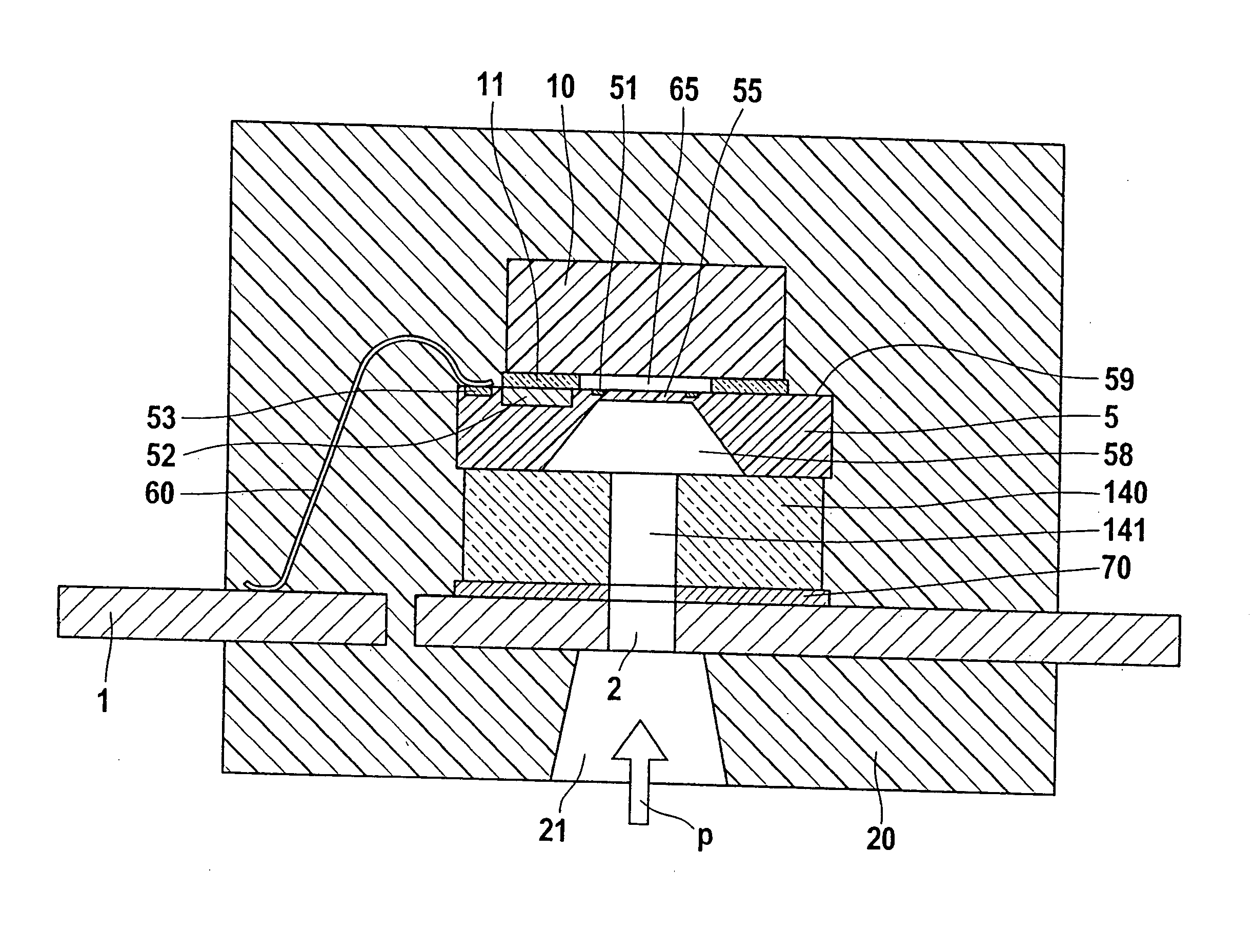
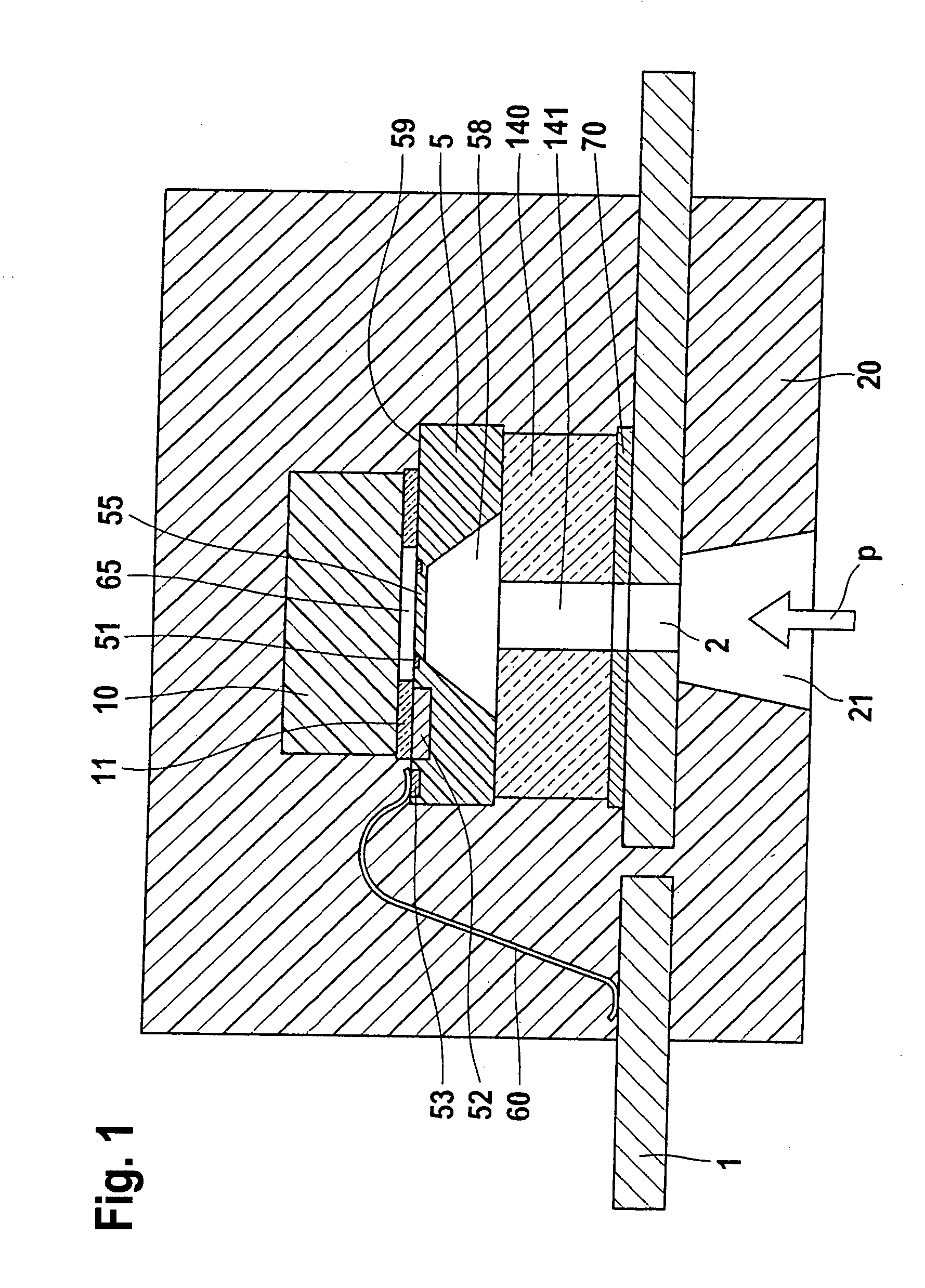
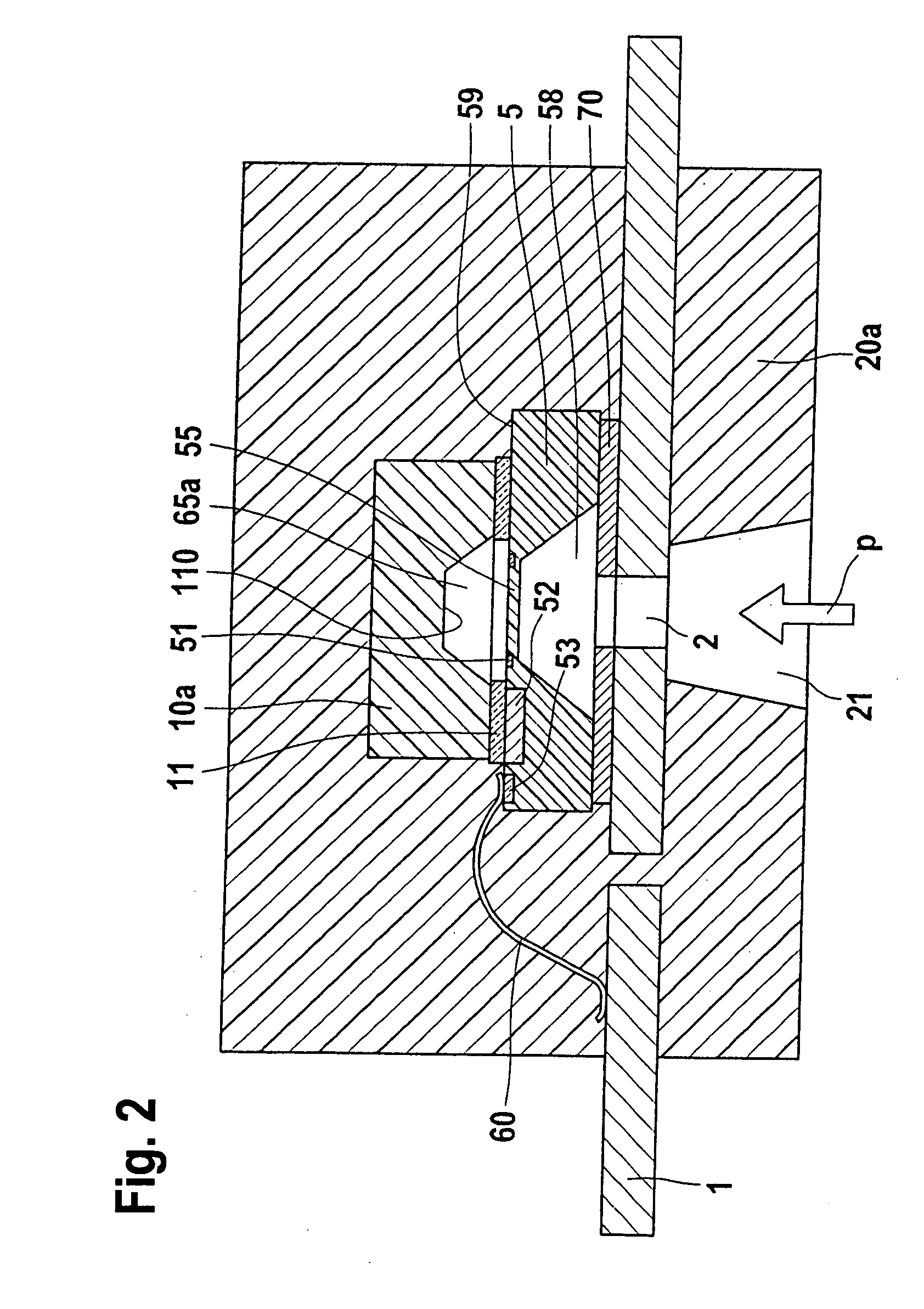
[0045]FIG. 1 shows a first specific embodiment of an example method according to the present invention for packaging semiconductor chips and a corresponding semiconductor chip system in a cross-sectional view.

[0046] In FIG. 1, reference numeral 1 denotes a leadframe on which a sensor chip 5, having a diaphragm region 55 and piezoresistors 51 located therein, is mounted via a glass base 140 and a solder layer 70. A cap 10 made of silicon is secured by a sealing glass layer 11 on sensor chip 5 in the periphery of diaphragm region 55. In the present example, sealing glass layer 11 is situated directly over integrated circuit 52 in sensor chip 5. A hollow space 65 is provided between cap 10 and diaphragm region 55. Reference numeral 53 denotes a bonding pad of an integrated circuit 52, the bonding pad being situated on a side edge region 59 of sensor chip 5 projec...


PUM

PropertyMeasurementUnit
areaaaaaaaaaaa
widthaaaaaaaaaa
mechanical stressaaaaaaaaaa

Abstract

A method for packaging semiconductor chips and a corresponding semiconductor chip system. The method includes making available a semiconductor chip having a diaphragm region; providing a cap over the diaphragm region, while leaving the diaphragm region open; mounting the semiconductor chip on a support frame; and providing a molded housing around the semiconductor chip and at least a partial region of the support frame for packaging the semiconductor chip.

Description

FIELD OF THE INVENTION [0001] The present invention relates to a method for packaging semiconductor chips and a corresponding semiconductor chip system. BACKGROUND INFORMATION [0002] Although applicable to any semiconductor chip systems, the present invention as well as the problem underlying it are explained with respect to a micromechanical semiconductor chip system having a pressure sensor. [0003]FIG. 9 shows an example of a method for packaging semiconductor chips and a corresponding semiconductor chip system in a cross-sectional view. [0004] In FIG. 9, reference numeral 100 denotes a TO8 base produced, for example, from Kovar. Reference numeral 5 is a micromechanical silicon pressure-sensor chip having piezoresistive transducer elements 51 that are accommodated on a diaphragm 55. To produce diaphragm 55, a cavity 58 is introduced onto the back of respective silicon pressure-sensor chip 5, for instance, by anisotropic etching, e.g., using KOH or TMAH. Alternatively, diaphragm 55...

Claims


Application Information

Patent Timeline
Patent Type & Authority Applications(United States)
IPC IPC(8): H01L23/02B81B3/00B81B7/00B81C1/00B81C3/00G01L9/00G01P1/02H01L21/50H01L21/52H01L21/56H01L21/60
CPCB81B7/0051G01L19/141G01P1/023H01L2224/48091H01L2224/48247H01L2924/01068H01L2924/0102H01L2924/01079H01L2924/1815B81C2203/0154H01L2224/48472H01L2924/00014H01L2924/00H01L2924/181H01L2224/05554H01L2924/15151H01L2224/73265H01L2924/00012H01L2224/32245
Inventor WEIBLEN, KURTBENZEL, HUBERTPINTER, STEFANGUENSCHEL, ROLANDHAAG, FRIEDER
Owner ROBERT BOSCH GMBH
Why Eureka
Try Eureka