
Semiconductor device featuring multi-layered electrode structure

a technology of semiconductor devices and electrode structures, which is applied in the direction of semiconductor devices, semiconductor/solid-state device details, electrical apparatus, etc., can solve the problems of fine silicon dioxide layer not being used as the gate insulating layer in mos, deterioration of the characteristic of the gate insulating layer, and impurities in the high-k gate insulating layer

Inactive Publication Date: 2005-09-01
NEC ELECTRONICS CORP
View PDF5 Cites 15 Cited by
  • Summary
  • Abstract
  • Description
  • Claims
  • Application Information

AI Technical Summary

Benefits of technology

[0016] Therefore, a main object of the present invention is to provide a semiconductor device featuring an electrode structure, which includes a high-k insulating layer composed of a high-k material, and an electrode formed on the high-k insulating layer and composed of polycrystalline silicon, and which is constituted so as to be substantially free from the problems as discussed above.

Problems solved by technology

In this case, a part of the impurities included in the gate electrode may be diffused in the gate insulating layer, and thus the impurities may react with the silicon atoms included in the gate insulating layer or silicon dioxide layer, to thereby produce defects therein, resulting in deterioration of the characteristic of the gate insulating layer.
However, such a fine silicon dioxide layer can be no longer used as the gate insulating layer in a MOS transistor, because a tunnel current, caused when a bias voltage applied to the gate electrode, has a magnitude which cannot be ignored with respect to a source / drain current.
Although further advances in the miniaturization and integration of semiconductor devices are possible by using a high-k gate insulating layer composed of one of the aforesaid high-k materials, there is still the problem that the diffusion of the impurities in the high-k gate insulating layer must be suppressed when the impurities are implanted and diffused in the gate electrode to thereby diminish resistance of the gate electrode.
In addition, another problem to be solved occurs when the high-k gate insulating layer is used.
In particular, aluminum elements or rare earth elements included in the high-k gate insulating layer may easily react with the silicon elements included in the polycrystalline silicon gate electrode, to thereby produce trap sites in the high-k gate insulating layer, resulting in considerable deterioration of the reliability and performance of the MOS transistor, as discussed in detail hereinafter.

Method used


Image

  • Semiconductor device featuring multi-layered electrode structure
  • Semiconductor device featuring multi-layered electrode structure
  • Semiconductor device featuring multi-layered electrode structure

Examples


first embodiment

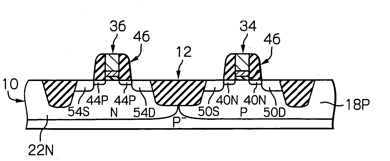
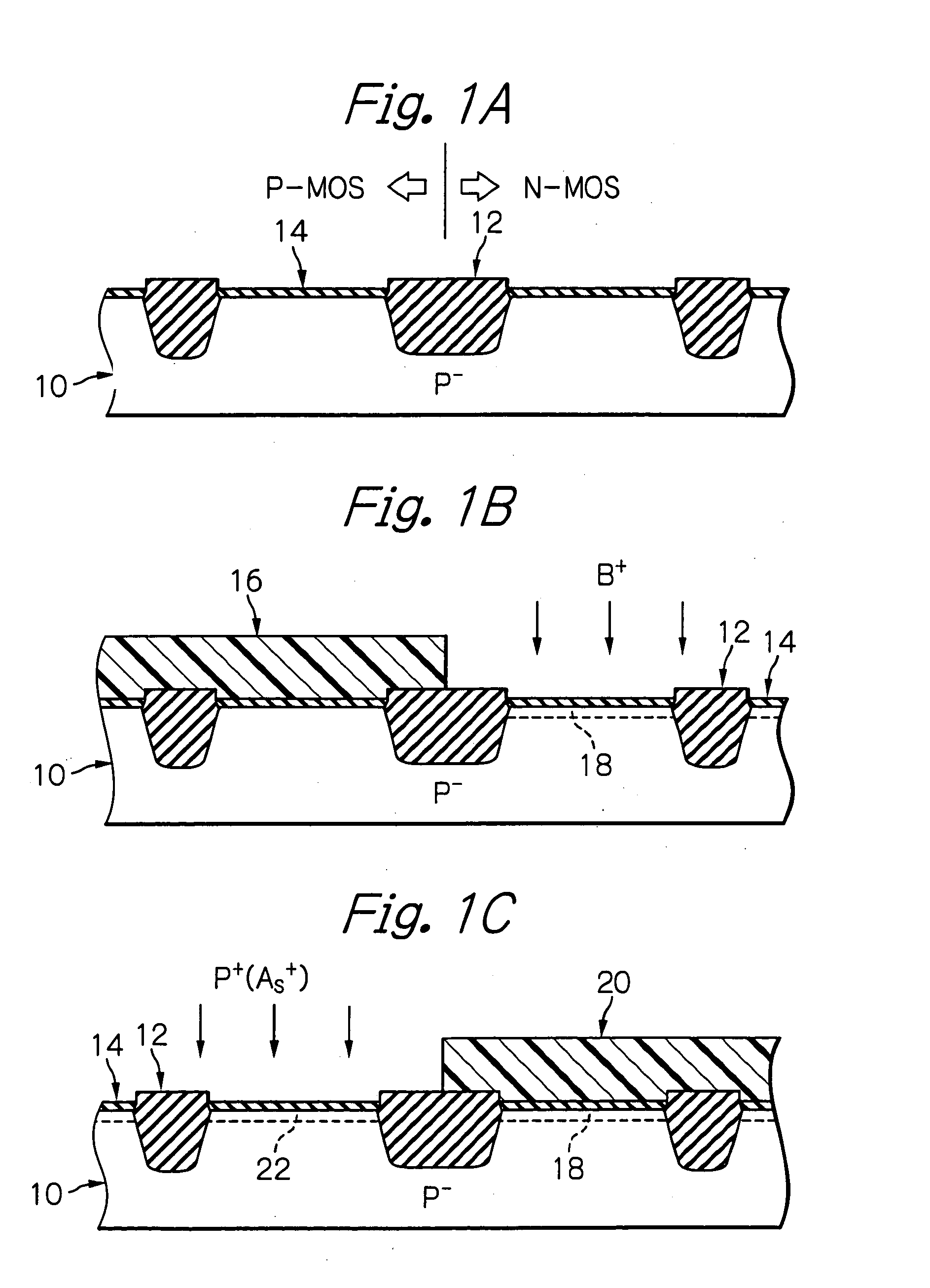
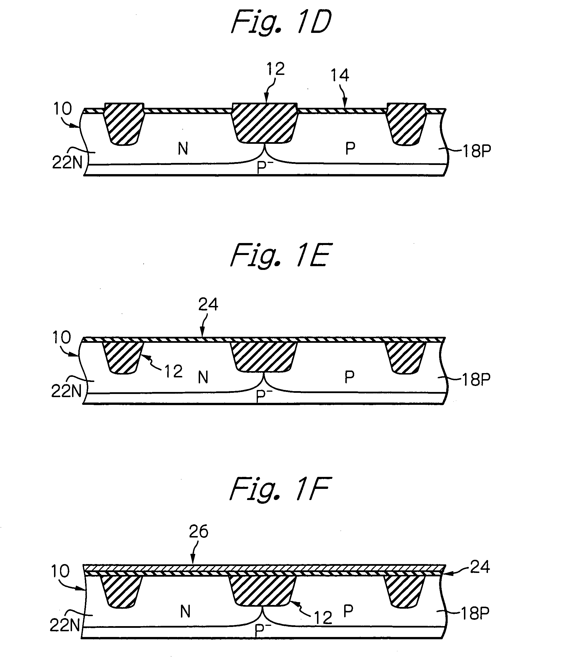
[0052] With reference to FIGS. 1A to 1N and FIGS. 1P to 1S, a production process for manufacturing a semiconductor device featuring a complementary MOS transistor according to the present invention will be now explained.

[0053] First, as shown in FIG. 1A, a p−-type semiconductor substrate 10, which is derived from, for example, a p−-type monocrystalline silicon wafer, is prepared. A surface of the semiconductor substrate 10 is sectioned into a plurality of chip areas by forming scribe lines therein, and a part of one chip area is illustrated in a cross sectional in FIG. 1A. In this drawing, reference 12 generally indicates an element-isolation layer, which is formed in the chip area concerned, by using a STI (shallow-trench isolation) method, such that a P-channel type MOS transistor-formation area “P-MOS” and an N-channel type MOS transistor-formation area “N-MOS” are defined on the surface of the chip area. Also, the semiconductor substrate 10 is already subjected to a thermal oxid...

second embodiment

[0137] Next, with reference to FIGS. 9A to 9D, a production process for manufacturing a semiconductor device featuring a complementary MOS transistor according to the present invention is explained below.

[0138] In FIG. 9A, reference 56 indicates a p−-type semiconductor substrate, which is derived from, for example, a p−-type monocrystalline silicon wafer. Similar to the aforesaid semiconductor substrate 10, a surface of the semiconductor substrate 56 is sectioned into a plurality of chip areas by forming scribe lines therein, and a part of one chip area is illustrated in a cross sectional in FIG. 9A. In this drawing, reference 58 generally indicates an element-isolation layer, which formed in the chip area concerned, by using a STI (shallow-trench isolation) method, such that a P-channel type MOS transistor-formation area “P-MOS” and an N-channel type MOS transistor-formation area “N-MOS” are defined on the surface of the chip area.

[0139] The semiconductor substrate 56 is already p...


PUM


Abstract

In a semiconductor device including a semiconductor substrate (10; 56), at least one electrode structure (34, 36; 72, 74) is provided on a surface of the semiconductor substrate. The electrode structure is constructed as a multi-layered electrode structure including an insulating layer (34A, 36A; 72A, 74A) formed on the surface of the semiconductor substrate and composed of a dielectric material exhibiting a dielectric constant larger than that of silicon dioxide, a lower electrode layer (34B, 36B; 72B, 74B) formed on the insulating layer and composed of polycrystalline silicon, and an upper electrode layer (34C, 36C; 72D, 74D) formed on the lower electrode layer and composed of polycrystalline silicon. The lower electrode layer features an average grain size of polycrystalline silicon which is larger than that of polycrystalline silicon of the upper electrode layer.

Description

BACKGROUND OF THE INVENTION [0001] 1. Field of the Invention [0002] The present invention relates to a semiconductor device featuring an electrode structure which includes an insulating layer, and an electrode formed on the insulating layer, and more particularly relates to a semiconductor device including metal oxide semiconductor (MOS) transistors, a dynamic random access memory (DRAM) device, a nonvolatile semiconductor memory device, and so on, each of which features such an electrode structure. [0003] 2. Description of the Related Art [0004] For example, a MOS transistor, included in a semiconductor device, features an electrode structure, which is referred to as a gate electrode structure. In this MOS transistor, a source region and a drain region are produced in, for example, a silicon substrate, which is usually derived from a monocrystalline silicon wafer, and the gate electrode structure is constructed on the silicon substrate so as to be associated with the source and dra...

Claims


Application Information

Patent Timeline
Patent Type & Authority Applications(United States)
IPC IPC(8): H01L21/28H01L21/336H01L21/8234H01L21/8238H01L23/485H01L27/088H01L27/092H01L29/40H01L29/423H01L29/49H01L29/51H01L29/78H10B12/00
CPCH01L21/2807H01L21/823842H01L21/823857H01L29/518H01L2924/0002H01L29/6659H01L2924/00
Inventor MASUOKA, YURIKIMIZUKA, NAOHIKO
Owner NEC ELECTRONICS CORP
Learn More