Filter circuit device and method of manufacturing the same

a filter circuit and filter element technology, applied in the field of filter circuit devices, can solve the problems of limited area saving, and achieve the effects of reducing the length of each pair of lines constituting the filter element, reducing the thickness of the filter element, and reducing the width of the filter elemen

Inactive Publication Date: 2005-09-01
SONY CORP
View PDF4 Cites 27 Cited by
  • Summary
  • Abstract
  • Description
  • Claims
  • Application Information

AI Technical Summary

Benefits of technology

[0015] It is another object of the present invention to provide a filter circuit device in which deterioration in filter characteristic is prevented and in which the occupied area of a filter element is reduced to realize miniaturization, and a method for manufacturing the same.
[0017] In the filter circuit device according to the present invention, since the first filter line as the high-impedance line of the filter element is formed by the thin film forming technique so as to have a significantly smaller thickness and a significantly smaller width than the second filter line as the low-impedance line formed by the thick film forming technique, the ratio of impedance between the high-impedance line and the low-impedance line can be increased and the length of each pair of lines formed in the wiring layers of the circuit layers can be significantly reduced.
[0020] In the method for manufacturing a filter circuit device according to the present invention, since the first filter line as the high-impedance line of the filter element is formed by the thin film forming technique so as to have a significantly smaller thickness and a significantly smaller width than the second filter line as the low-impedance line formed by the thick film forming technique, the ratio of impedance between the high-impedance line and the low-impedance line can be increased and the length of each pair of lines constituting the filter element can be significantly reduced. Thus, a further miniaturized filter circuit device can be manufactured.
[0021] In this method for manufacturing a filter circuit device, since the high-impedance line of the filter element is formed by the thin film forming technique, the high-impedance line having a smaller thickness and less unevenness in size than when it is formed by the thick film forming technique can be formed with high accuracy. Therefore, a filter circuit device having a filter element in which deterioration in filter characteristic is prevented is manufactured at a high yield.

Problems solved by technology

Therefore, area-saving is limited.

Method used


Image

  • Filter circuit device and method of manufacturing the same
  • Filter circuit device and method of manufacturing the same
  • Filter circuit device and method of manufacturing the same

Examples


Embodiment Construction

[0036] An embodiment of the present invention will now be described in detail with reference to the drawings.

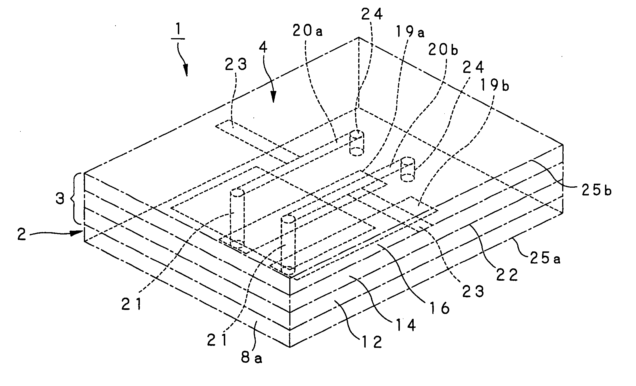
[0037] A filter circuit device to which the present invention is applied constitutes a high-frequency circuit used in a transmitting / receiving unit provided in a portable communication terminal device or the like and adapted for processing a high-frequency signal. The filter circuit device 1 has a first circuit part 2, a second circuit part 3 formed on a major surface (hereinafter referred to as forming surface) 2a of the first circuit part 2, and a filter element 4 formed to extend onto the first circuit part 2 and the second circuit part 3, as shown in FIGS. 4 and 5.

[0038] In the filter circuit device 1, the first circuit part 2 has a wiring part of a power system and a control system with respect to the second circuit part 3 formed on the forming surface 2a, and a mounting surface 2b with respect to a base board 90. In the filter circuit device 1, a semiconductor compone...


PUM


Abstract

This invention is a filter circuit having a filter element. A filter element (4) is a parallel resonator circuit including a pair of first resonator lines (19a) (19b) formed by a thick film forming technique and a pair of second resonator lines (20a) (20b). As the thickness of the pair of second resonator lines (20a) (20b) is significantly reduced, the impedance ratio between the pair of second resonator lines (20a) (20b) and the pair of first resonator lines (19a) (19b) is increased. Therefore, the length of these pairs of resonator lines (19a) (19b) (20a) (20b) is reduced and miniaturization of the filter element is realized.

Description

TECHNICAL FIELD [0001] This invention relates to a filter circuit device having a filter element and a method for manufacturing the same. [0002] This application claims priority of Japanese Patent Application No. 2001-397677, filed on Dec. 27, 2001, the entirety of which is incorporated by reference herein. BACKGROUND ART [0003] Recently, in high-frequency applications using a microwave band or a milliwave band as a carrier, for example, in wireless LAN or various communication terminals, reduction in size and thickness of equipment and circuit board has been demanded. In a circuit board for such high-frequency applications, filter elements such as a low-pass filter (LPF), a high-pass filter (HPF) and a band-pass filter (BPF) are designed with a distributed constant, for example, using a microstrip line or a strip line that enables relatively high space-saving, instead of using a lumped constant design using chip components like an inductor and a capacitor. [0004] For example, a cir...

Claims


Application Information

Patent Timeline
Patent Type & Authority Applications(United States)
IPC IPC(8): H05K3/46H01P1/203H01P3/08H01P7/08H05K1/16H05K3/02
CPCH01P1/203H01P1/20345H05K1/16H05K2201/1006H05K3/4644H05K2201/0352H05K2201/09236H05K3/02H01L2224/16225H01L2924/15184H01L2924/16152H01P3/08H01P7/08
Inventor HIRABAYASHI, TAKAYUKI
Owner SONY CORP
Why Eureka
Try Eureka