

Method of and apparatus for producing micro lens and micro lens
a micro lens and micro-lens technology, applied in the field of micro lens and micro-lens, can solve the problems of difficult to form a curved surface, difficult to uniformly apply the lens material, and increase so as to achieve the effect of minimizing the fluctuation in shape and high accuracy
- Summary
- Abstract
- Description
- Claims
- Application Information
AI Technical Summary
Benefits of technology
Problems solved by technology
Method used
Image

Examples
first embodiment
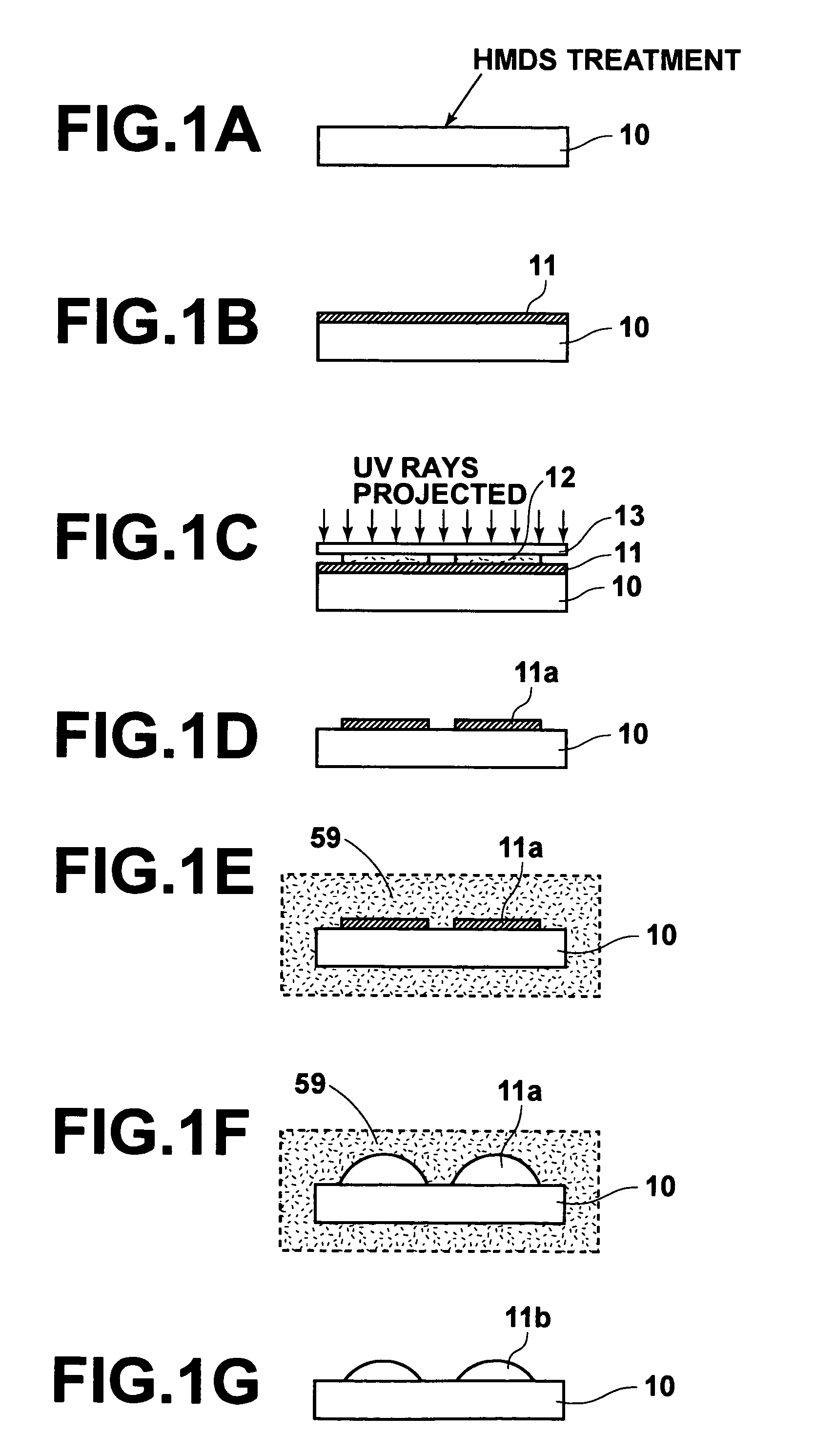
[0069] A method of producing a micro lens in accordance with a first embodiment of the present invention will be described with reference to FIGS. 1A to 1G, hereinbelow. A surface of a transparent SiO2 glass substrate 10 is treated with HMDS (hexamethyldisilazane) as shown in FIG. 1A. Then the surface of the substrate 10 is coated with positive resist 11 of phenolic novolak series in a predetermined thickness by spin coating as shown in FIG. 1B. The thickness t of the resist 11 is defined by formula t=a·V / S wherein V represents the desired volume of the lens, S represents the area of a cross-section defined by a desired curved surface of the lens and the substrate surface, and a represents a constant determined by the process, and is controlled by coating conditions such as the viscosity of the resist and the rotational speed of the spin coating.
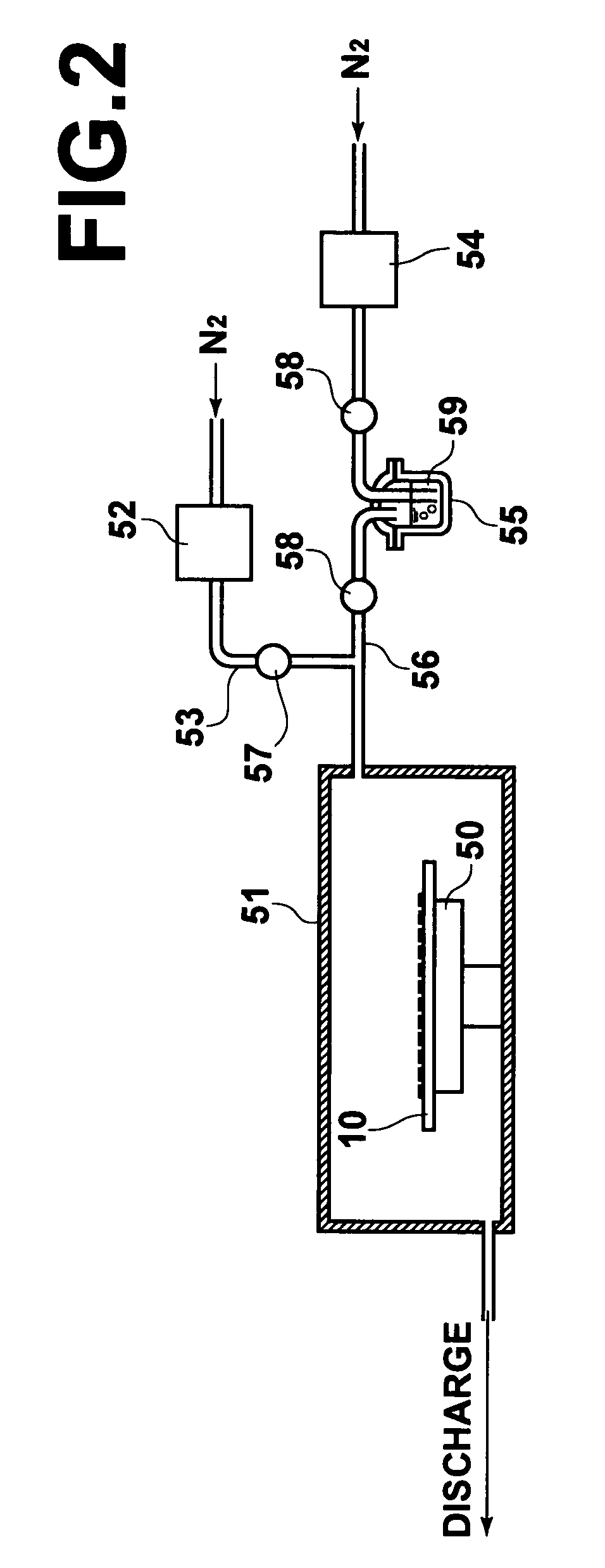
[0070] Then the substrate 10 thus treated is soft-baked for a predetermined time at 80 to 120° C. by the use of a hot plate or a clean ove...
second embodiment
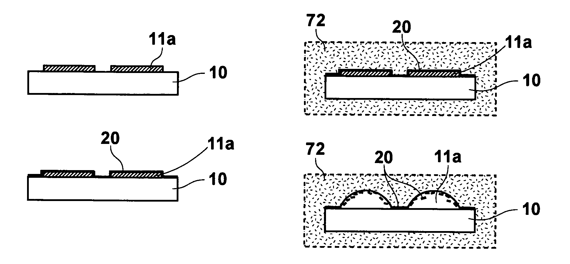
[0088] A method of producing a micro lens in accordance with a second embodiment of the present invention will be described with reference to FIGS. 4A to 4F, hereinbelow. A resist pattern 11a of phenolic novolak series is formed on a SiO2 glass substrate 10 in the same manner as in the first embodiment described above as shown in FIG. 4A. That is, FIG. 4A corresponds to FIG. 1D.
[0089] Then the surface of the substrate 10 on which the resist pattern 11a has been formed is treated with oxygen plasma. In this embodiment, descum ashing is carried out with a plane-parallel plate oxygen plasma ashing apparatus. The treating conditions are, for instance, as follows.
high frequency power:10 to 50 W, treating time:10 to 60 s, chamber pressure:1 to 30 Pa
[0090] Next, the surface of the substrate 10 is coated with liquid repellent coating. In this embodiment, a silane coupling agent of fluorocarbon series (Optool DSX: Daikin Industries, Ltd.) is employed as the coating material, and the liqu...
third embodiment
[0102] A method of producing a micro lens in accordance with a third embodiment of the present invention will be described with reference to FIGS. 6A to 6C, hereinbelow. In this embodiment, the shape of lens-like portions formed on a substrate is transferred to the substrate and micro lenses of the same material as the substrate are formed on the substrate.
[0103] A transparent SiO2 glass substrate 10 on which micro lenses 11b are formed is first prepared by the method described above in the first or second embodiment. In this embodiment, the solidifying treatment at high temperature on the micro lenses 11b need not be necessarily carried out. Though referred to as “the micro lenses 11b” here, since it is not necessary for the lens-like portions formed on the substrate 10 to operate as lenses, the lens-like portions may be formed by opaque resin.
[0104] The substrate 10 is set to an induction coupling plasma etching apparatus (ICP) and anisotropic etching is carried out thereon. As ...
PUM
 Abstract
Description
Claims
Application Information