Substrate processing method and apparatus

a processing method and substrate technology, applied in the direction of manufacturing tools, grinding machine components, lapping machines, etc., can solve the problems of insufficient polishing of substrate local areas, inability and difficulty in polishing native oxides. to achieve uniform planarization

Inactive Publication Date: 2005-09-01
EBARA CORP
View PDF4 Cites 30 Cited by
  • Summary
  • Abstract
  • Description
  • Claims
  • Application Information

AI Technical Summary

Benefits of technology

[0008] The present invention has been made in view of the above drawbacks. It is, therefore, an object of the present invention to provide a substrate processing method and appara

Problems solved by technology

Further, the native oxide is more difficult to polish than the complex.
Accordingly, when the native oxide is formed so as to have uneven film t

Method used


Image

  • Substrate processing method and apparatus
  • Substrate processing method and apparatus
  • Substrate processing method and apparatus

Examples


first embodiment

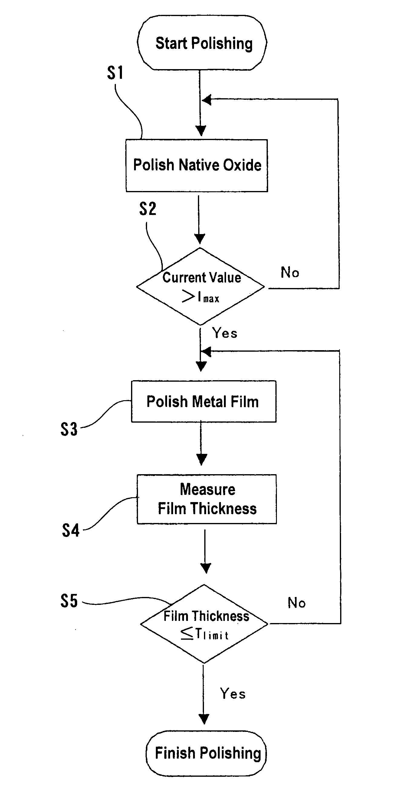
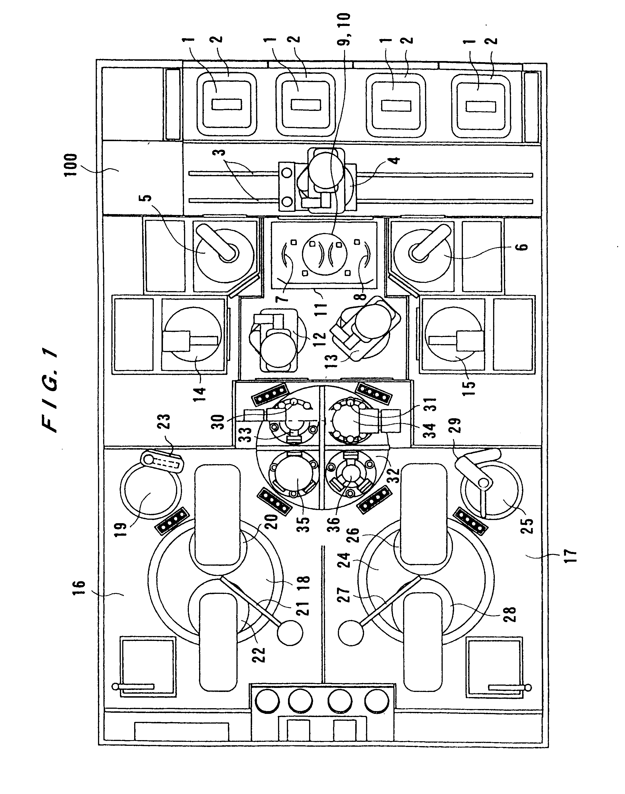
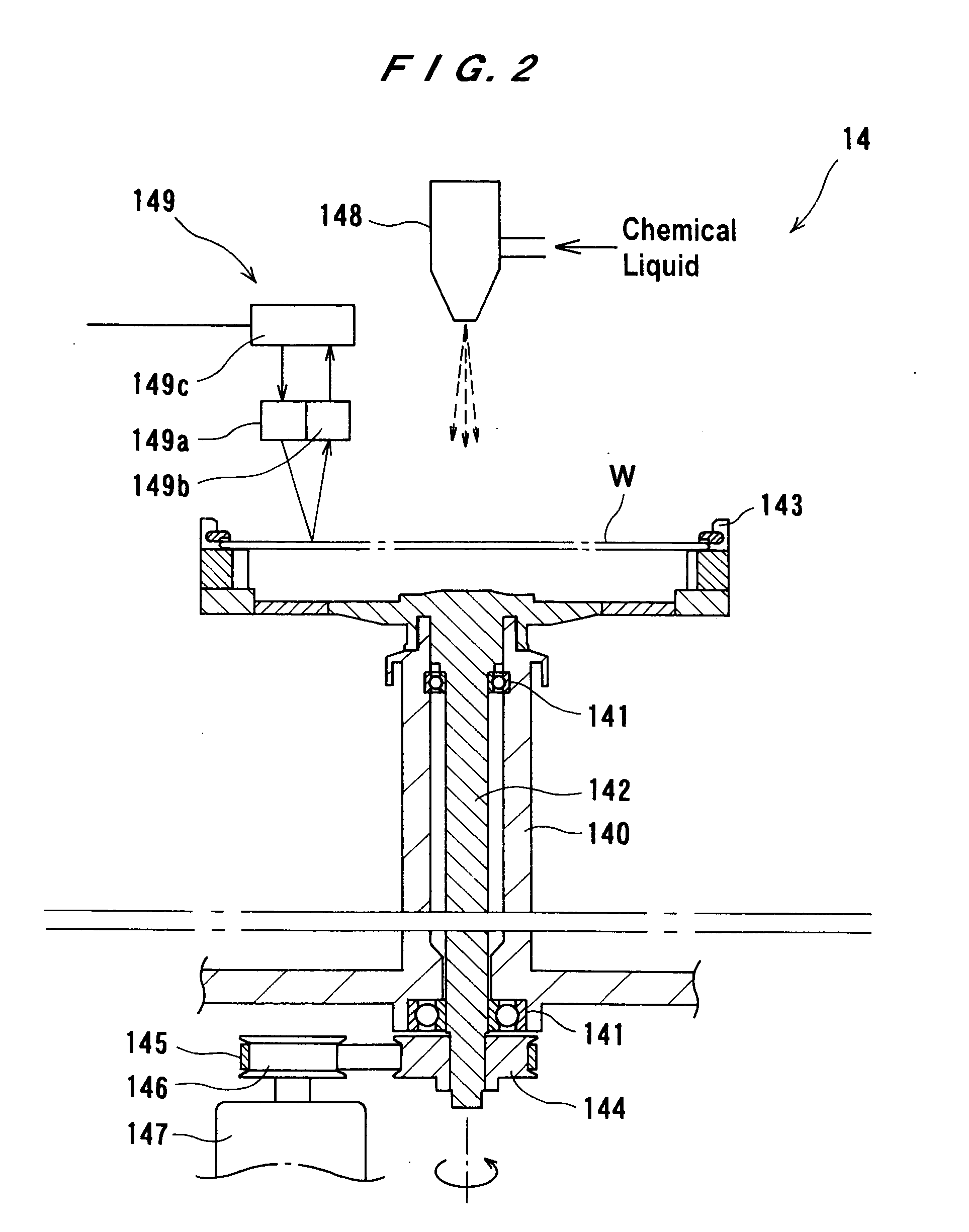
[0042]FIG. 1 is a plan view showing a polishing apparatus as a substrate processing apparatus according to the present invention. As shown in FIG. 1, the polishing apparatus has four loading / unloading stages 2 on which wafer cassettes 1 are placed. Each of the wafer cassettes 1 stocks a large number of semiconductor wafers therein. The polishing apparatus includes a moving mechanism 3 arranged along an array of the loading / unloading stages 2. The moving mechanism 3 includes a first transfer robot 4 having two hands. Further, the polishing apparatus has a film thickness measurement unit 100 adjacent to the moving mechanism 3. The first transfer robot 4 is accessible to each of the wafer cassettes 1 placed on the loading / unloading stages 2 and to the film thickness measurement unit 100.

[0043] The polishing apparatus also includes two cleaning and drying devices 5 and 6 disposed at an opposite side of the moving mechanism 3 to the wafer cassettes 1. The hands of the first transfer robo...

second embodiment

[0067]FIG. 4 is a plan view showing a polishing apparatus as a substrate processing apparatus according to the present invention. As shown in FIG. 4, the polishing apparatus has a loading / unloading stage 2 on which wafer cassettes 1 are placed, a first transfer robot 201 having a hand accessible to the wafer cassettes 1, wafer stages 202 and 203 provided on both sides of the first transfer robot 201, and a vacuum chamber 204 arranged along an array of the first transfer robot 201 and the wafer stages 202 and 203.

[0068] The vacuum chamber 204 houses a dry process unit 206, a second transfer robot 205 having a hand accessible to the wafer stage 202, and a third transfer robot 207 having a hand accessible to the wafer stage 203. In the present embodiment, the dry process unit 206 comprises a dry etching unit for reducing or etching a native oxide of a metal film formed on a surface of a wafer. The vacuum chamber 204 includes a shutter 208 disposed between the second transfer robot 205 ...


PUM


Abstract

A substrate processing apparatus can process a substrate having a metal film formed thereon. The substrate processing apparatus has a process unit configured to remove a native oxide of a metal film formed on a surface of a substrate. The substrate processing apparatus also has a planarization unit configured to planarize the metal film of the substrate. The process unit may comprise a wet process unit configured to dissolve the native oxide of the metal film in a chemical liquid or a dry process unit configured to reduce or etch the native oxide of the metal film with a gas.

Description

BACKGROUND OF THE INVENTION [0001] 1. Field of the Invention [0002] The present invention relates to a substrate processing method and apparatus, and more particularly to a substrate processing method and apparatus for polishing a substrate such as a semiconductor wafer to a flat mirror finish. [0003] 2. Description of the Related Art [0004] As semiconductor devices have become more highly integrated in recent years, circuit interconnections have become finer and distances between those circuit interconnections have become smaller. In the case of photolithography, which can form interconnections that are at most 0.5 μm wide, it is required that surfaces on which pattern images are to be focused by a stepper should be as flat as possible because the depth of focus of an optical system is relatively small. In order to planarize such a semiconductor wafer, there has been used a polishing apparatus for performing chemical mechanical polishing (CMP). [0005] This type of chemical mechanic...

Claims


Application Information

Patent Timeline
IPC IPC(8): B24B37/04B24B49/12B24B49/16H01L21/00H01L21/321
CPCB24B37/013B24B49/12B24B49/16H01L21/67219H01L21/6708H01L21/67173H01L21/3212
Inventor FUKUNAGA, AKIRANOMURA, TOSHIKAZUTOKUSHIGE, KATSUHIKOTSUJIMURA, MANABU
Owner EBARA CORP
Why Eureka
Try Eureka