Method of forming dual damascene structures

a damascene and structure technology, applied in the direction of basic electric elements, semiconductor/solid-state device manufacturing, electric devices, etc., can solve the problems of square root2 times of accumulative alignment error, tendency to occur via to trench bridging phenomenon, etc., to improve production yield rate, improve alignment accuracy, and reduce the noise of alignment signals

Inactive Publication Date: 2005-09-08
UNITED MICROELECTRONICS CORP
View PDF8 Cites 29 Cited by
  • Summary
  • Abstract
  • Description
  • Claims
  • Application Information

AI Technical Summary

Benefits of technology

[0018] It is an advantage of the present invention that the present invention method of forming the dual damascene copper wire is to form the composite layer or the bottom anti-reflective coating opaque to the alignment light beams. Therefore, the alignment light beams are prevented from reaching to the alignment mark in the second alignment process to achieve two direct alignments to improve alignment accuracy. The via to trench bridging phenomenon is thus avoided. The via to trench bridging margin is enlarged to avoid problems usually occurring in the prior art fabricating method which utilizes one direct

Problems solved by technology

As integrated circuit technology advances, improving the yield of the dual damascene structure, simplifying the process flow and reducing the production cost are important issues in the manufacturing process of integrated circuits at the present

Method used


Image

  • Method of forming dual damascene structures
  • Method of forming dual damascene structures
  • Method of forming dual damascene structures

Examples


Embodiment Construction

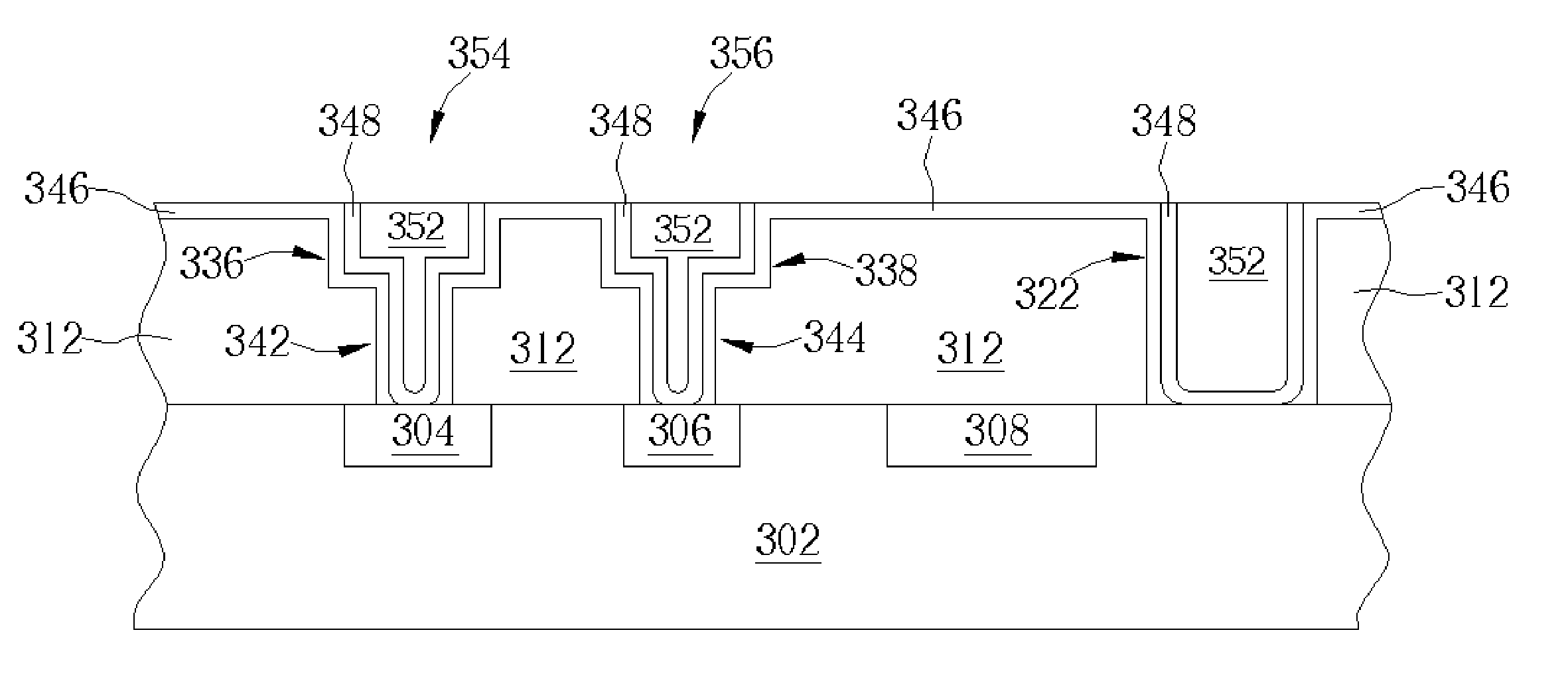
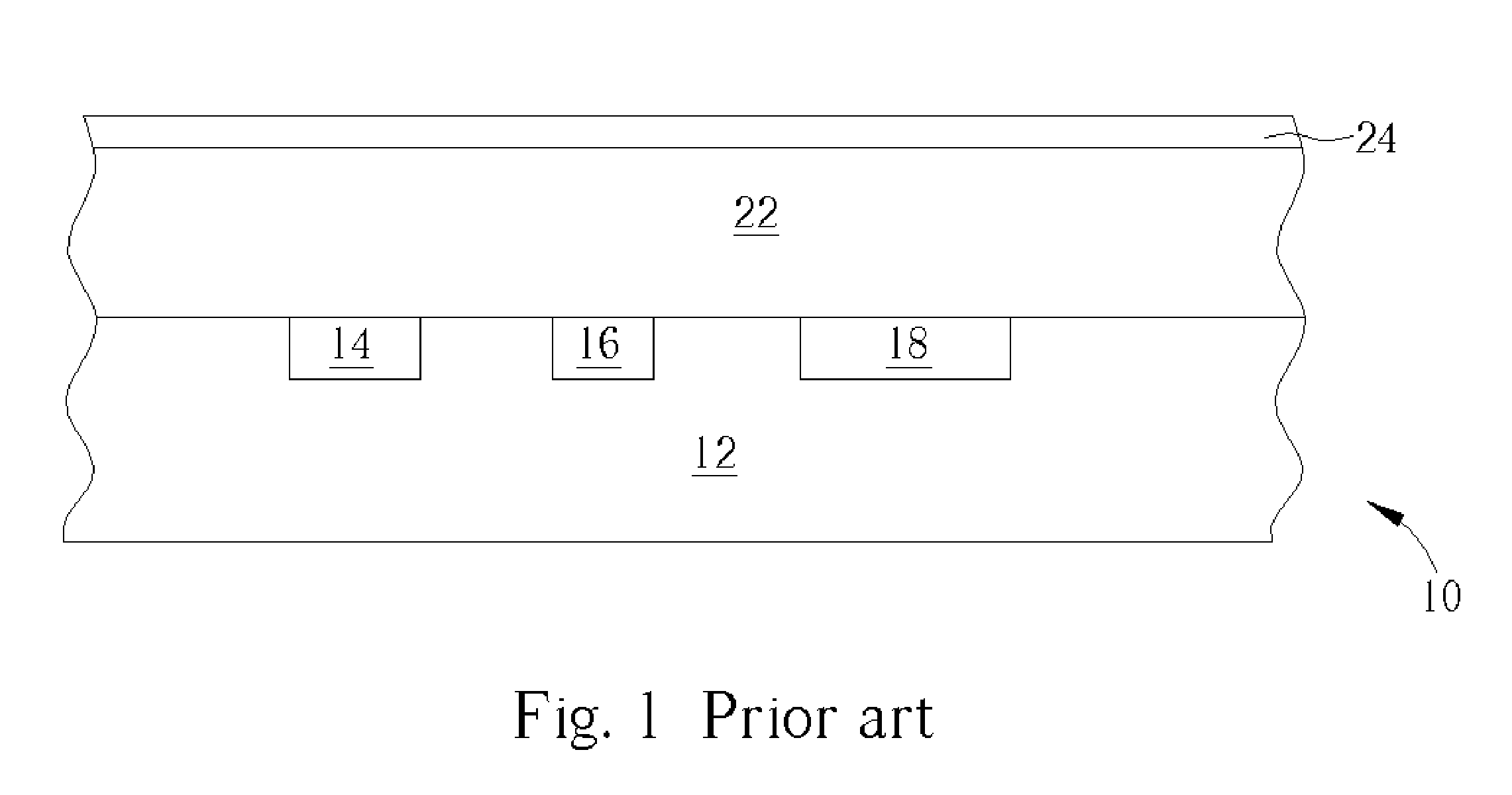
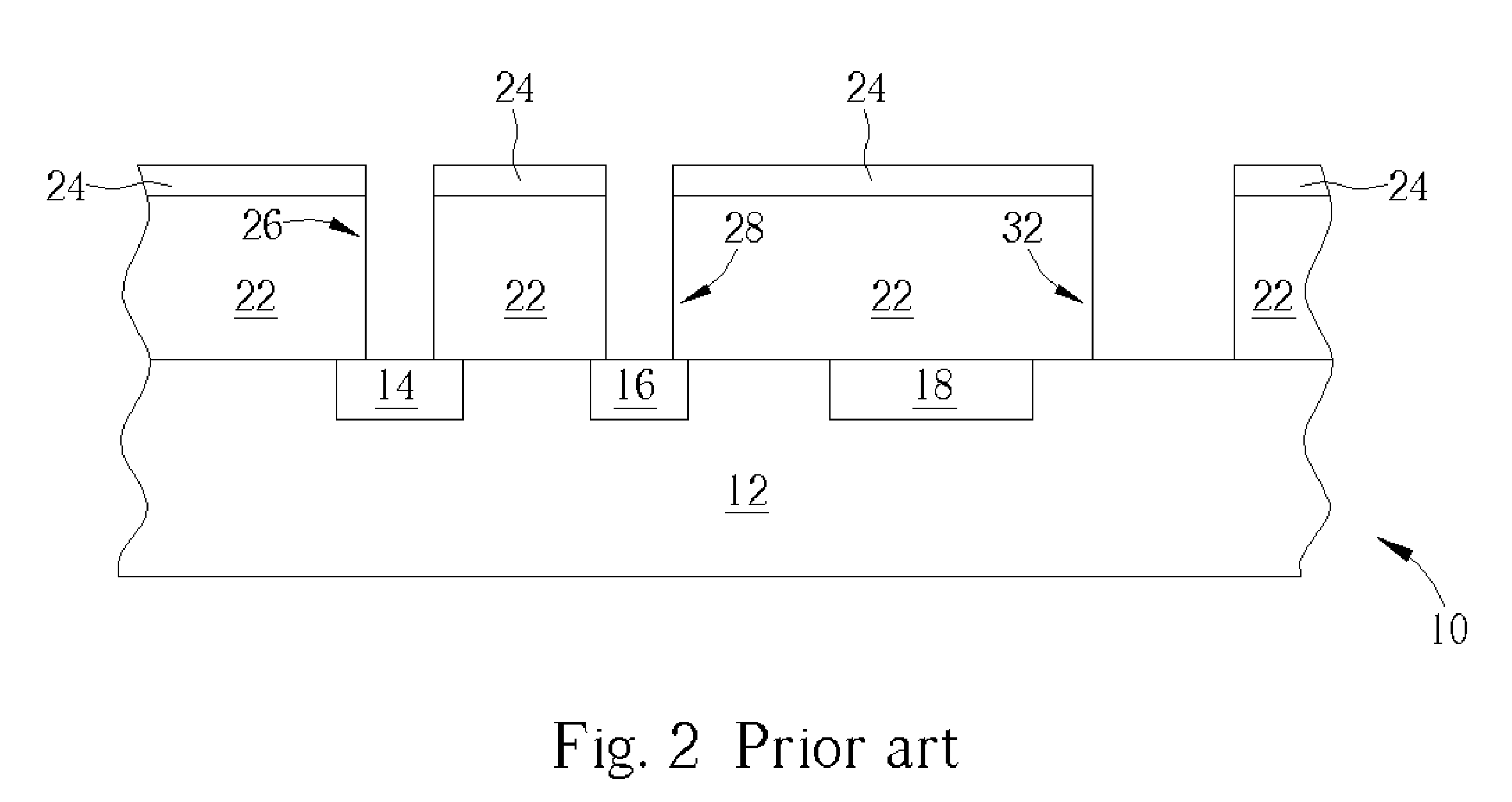
[0025] Please refer to FIG. 9 to FIG. 15. FIG. 9 to FIG. 15 are schematic diagrams of a method of fabricating dual damascene copper wires 154, 156 according to a first preferred embodiment of the present invention. As shown in FIG. 9, a semiconductor wafer 100 comprises a substrate 102, conductive layers 104, 106, 108 disposed on predefined regions of a surface of the substrate 102, and an inter layer dielectric 112 disposed on the surface of the substrate 102 and covering the conductive layers 104, 106, 108. Since the other elements disposed on the surface of the substrate 102 are not the concerning parts in the dual damascene process, they are not shown in FIG. 9 and in other figures. Each of the conductive layers 104, 106 may be a source of a transistor, a gate of a transistor, a drain of a transistor, a lower level wire, a landing pad, or a resistor, and the conductive layer 108 is an alignment mark.

[0026] A hard mask layer 114 is formed on a surface of the inter layer dielectr...


PUM


Abstract

A method of forming at least one wire on a substrate comprising at least one conductive region is provided. AnAn insulatingayer is disposed on the substrate. The method includes forming a hard mask layer on the insulating layer followed by forming at least one recess by removing portions of the hard mask layer and the insulating layer, forming a light blocking layer on the hard mask layer and the recess, and the light blocking layer and the hard mask layer forming a composite layer, forming a gap filling layer filling up the recess on the light blocking layer, forming a photoresist layer on the gap filling layer, aligning a photo mask with the recess by utilizing the composite layer as a mask, and performing an exposure/development process to form at least one pattern above the recess in the photoresist layer.

Description

BACKGROUND OF INVENTION [0001] 1. Field of the Invention [0002] The present invention relates to a method of forming dual damascene structures, and more particularly, to a method utilizing two direct alignments to form dual damascene structures having a large via to trench bridging margin. [0003] 2. Description of the Prior Art [0004] A dual damascene process is a method of forming a conductive wire coupled with a via plug in a dielectric layer. The dual damascene structure, comprising a trench and a via hole, is used to connect devices and wires in a semiconductor wafer within various layers and is isolated from other devices by the inter-layer dielectrics (ILD) around it. Since the resistivity of copper is smaller than the resistivity of aluminum (Al), a large current can be sustained in a small area. Consequently, chips having high speed, high integration, and high efficiency (with 30-40% improvement) are fabricated. To fill copper into the dual damascene structures thus becomes ...

Claims


Application Information

Patent Timeline
IPC IPC(8): H01L21/311H01L21/4763H01L21/76
CPCH01L21/31144H01L21/76846H01L21/76844H01L21/76808
Inventor LIN, BENJAMIN SZU-MINHUANG, SHOU-WAN
Owner UNITED MICROELECTRONICS CORP
Why Eureka
Try Eureka