
Method for manufacturing display device

a display device and manufacturing method technology, applied in the field of display devices, can solve the problems that the deterioration of the display device cannot be fully prevented, and achieve the effect of high reliability and preferable yield

Inactive Publication Date: 2005-09-08
SEMICON ENERGY LAB CO LTD
View PDF33 Cites 26 Cited by
  • Summary
  • Abstract
  • Description
  • Claims
  • Application Information

AI Technical Summary

Benefits of technology

[0006] It is an object of the present invention to provide a highly reliable display device which can prevent a light emitting element from deteriorating, and a method for manufacturing the display device more simply.
[0015] According to the invention, a display device in which degasification is not generated can be manufactured without increasing the number of steps; therefore, a light emitting element can be prevented from deteriorating. Hence, a highly reliable display device which can display a high-definition and high-quality image can be manufactured with a preferable yield.

Problems solved by technology

However, even when such measures are taken, the deterioration of an EL display device can not be fully prevented.

Method used


Image

  • Method for manufacturing display device
  • Method for manufacturing display device
  • Method for manufacturing display device

Examples


embodiment mode 1

[Embodiment Mode 1]

[0038] Embodiment Mode of the present invention will be described in detail with reference to the accompanying drawings. However, it is to be understood that the invention is not limited to the description below and various changes and modifications will be apparent to those skilled in the art, unless such changes and modifications depart from the content and scope of the invention. Therefore, the invention is not interpreted with limiting to the description in this embodiment mode. Note that the same reference numerals denote the same parts or parts having the same function in different drawings and the explanation will not be repeated in a constitution of the invention hereinafter explained.

[0039]FIG. 14A shows a top view of a structure of a display panel according to the invention. A pixel portion 2701 in which pixels 2702 are arranged in a matrix, a scanning line input terminal 2703, and a signal line input terminal 2704 are formed over a substrate 2700 havin...

embodiment mode 2

[Embodiment Mode 2]

[0119] In this embodiment mode, an example of a display device according to the present invention in which a connection structure of a first electrode and a wiring is different is described with reference to FIGS. 3A to 3D, and FIGS. 4A and 4B.

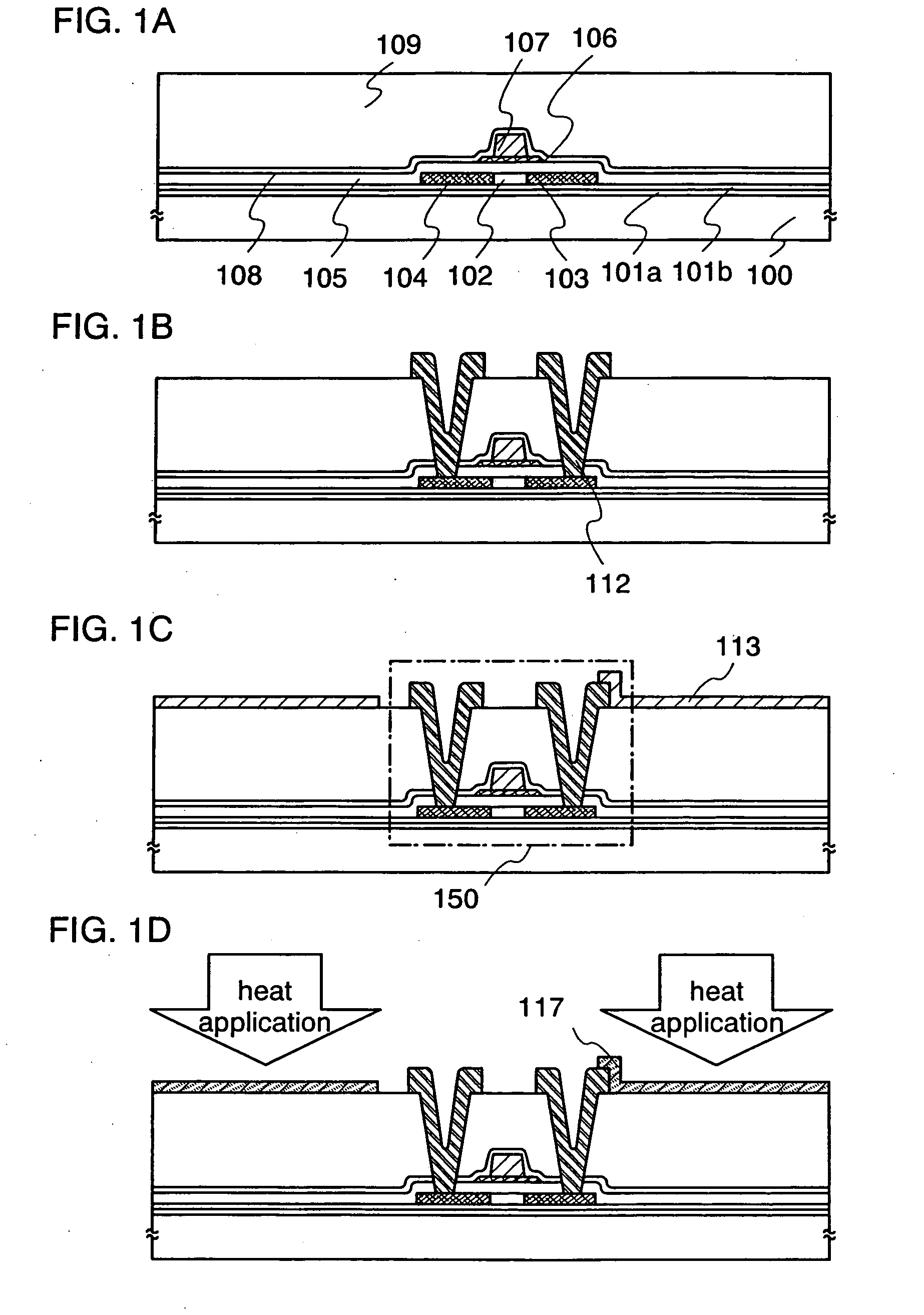
[0120] As shown in Embodiment Mode 1, base films 101a and 101b are formed over a substrate 100, and a semiconductor layer 102 having impurity regions 103 and 104 is formed. Conductive layers 106 and 107 which are gate electrodes are formed over the semiconductor layer 102 with a gate insulating film 105 therebetween, and an insulating film 108 is formed as a passivation film. Then, an insulating layer 109 is formed as an interlayer film (see FIG. 3A). In this embodiment mode, an insulating layer in which a skeleton is configured by the bond of silicon (Si) and oxygen (O) is used as the insulating layer 109.

[0121] In this embodiment mode, a first electrode 113 is selectively formed over the insulating layer 109 before formi...

embodiment mode 3

[Embodiment Mode 3]

[0127] In this embodiment mode, in a display device manufactured according to Embodiment Mode 1, examples of a dual emission type, a top emission type which is a one-side emission type are described with reference to FIGS. 6 and 7.

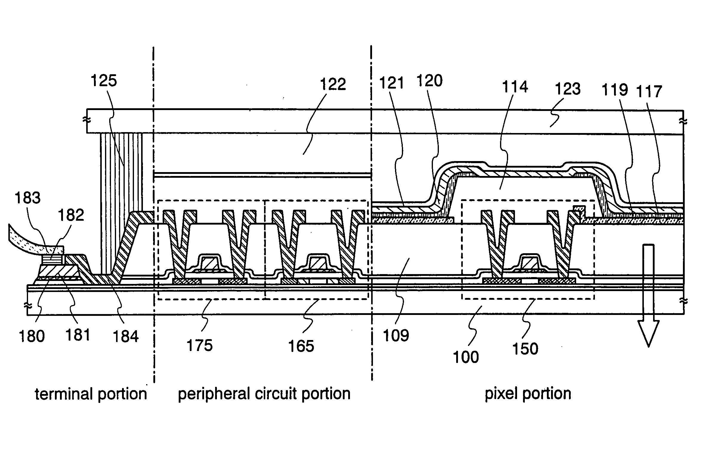
[0128] In FIG. 6, reference numeral 1300 denotes an element substrate; 1355, 1365 and 1375, TFTs; 1317, a first electrode; 1319, a light emitting layer; 1320, a second electrode; 1321, a transparent conductive film; 1322, a filler; 1325, a sealant; 1305, a gate insulating film; 1309, an insulating layer; 1314, a partition wall; 1323, a sealing substrate; 1384, a wiring layer; 1380 and 1381, terminal electrodes; 1382, an anisotropy conductive layer; and 1383, an FPC.

[0129] A display device shown in FIG. 6 is a dual emission type, and has a structure in which light is emitted in directions indicated by arrows, namely, to the both sides of the element substrate 1300 and the sealing substrate 1323. In this embodiment mode, a transparent co...


PUM

PropertyMeasurementUnit
temperatureaaaaaaaaaa
pressureaaaaaaaaaa
pressureaaaaaaaaaa

Abstract

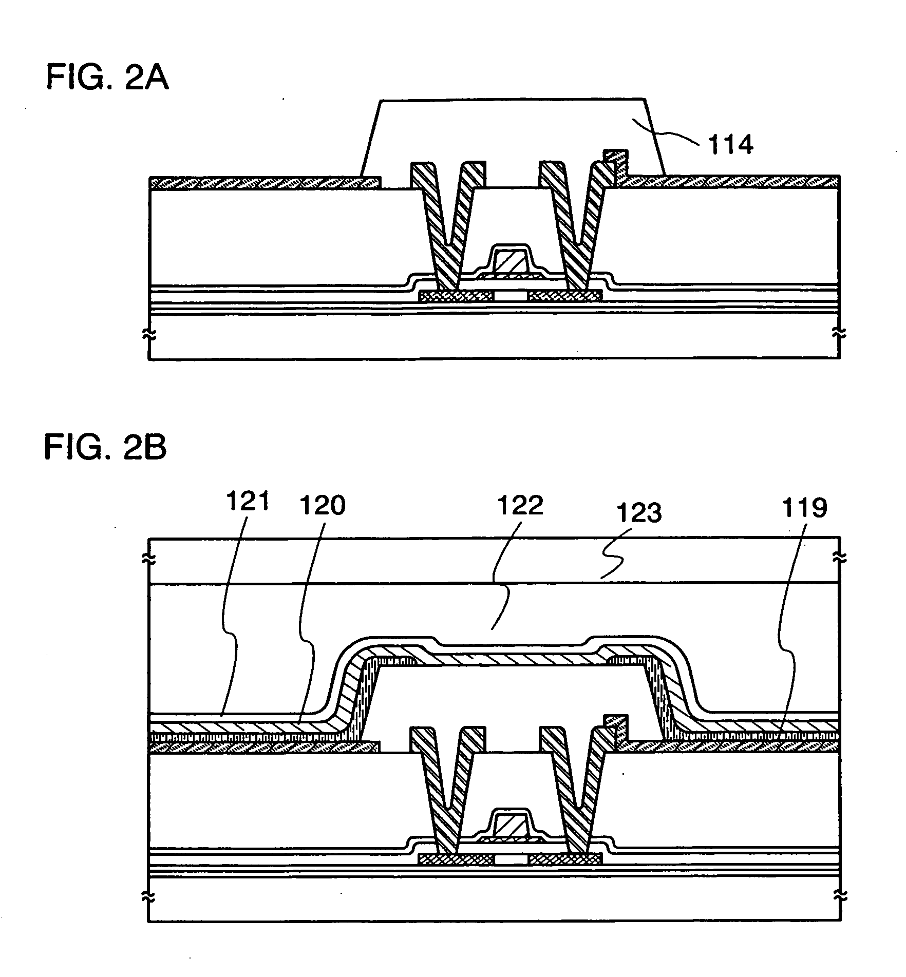
It is an object of the present invention to provide a method for manufacturing a highly reliable display device with a preferable yield. A method for manufacturing a display device according to the invention comprises the steps of: forming a first electrode including a conductive material added with a material which prevents crystallization; forming a layer containing an organic compound over the first electrode by heating the first electrode under a reduced pressure at temperatures of 350° C. or higher; and forming a second electrode over the layer containing an organic compound. It is preferable to perform the heat treatment at temperatures of 350° C. or higher, preferably, 375° C. or higher for 12 hours or longer. When the first electrode is formed by using indium tin oxide containing silicon oxide, a highly display device can be manufactured.

Description

BACKGROUND OF THE INVENTION [0001] 1. Field of the Invention [0002] The present invention relates to a display device that includes an element having a light emitting material sandwiched between electrodes (hereinafter referred to as a “light emitting element”), and to a manufacturing method of the display device. In particular, the invention relates to a display device using a light emitting material that generates EL (Electro Luminescence) (hereinafter also referred to as an “EL material”). [0003] 2. Description of the Related Art [0004] An EL material (particularly, an organic EL material) that mainly constitutes an EL element is characterized in that it is sensitive to moisture and degrades easily. Therefore, when an EL display device is manufactured, a technique for reducing the moisture content in the device is required. As its measures, a structure in which a drying agent is provided in an EL display device (an electroluminescence device) and then sealed (for example, Referen...

Claims


Application Information

Patent Timeline
Patent Type & Authority Applications(United States)
IPC IPC(8): H01J9/00H01J9/24
CPCH01L51/5206H01L27/3244H01L51/529H01L51/525H10K59/8723H10K59/131H10K59/8051H10K59/8794H10K50/81H10K59/12H10K50/87H10K50/8428
Inventor YAMAZAKI, SHUNPEITAKAYAMA, TORUAKIMOTO, KENGOTOKUNAGA, HAJIME
Owner SEMICON ENERGY LAB CO LTD
Learn More