Substrate holder which is self-adjusting for substrate deformation

a substrate and self-adjusting technology, applied in the field of substrate holders, can solve the problems of localized thermal expansion of the wafer, thermal distortion of the wafer, and incompatibility with vacuum chamber systems, and achieve the effect of accurate alignmen

Inactive Publication Date: 2005-09-15
APPLIED MATERIALS INC
View PDF9 Cites 12 Cited by
  • Summary
  • Abstract
  • Description
  • Claims
  • Application Information

AI Technical Summary

Benefits of technology

[0015] A microprocessor system utilizes the processing conditions and physical characteristics of the substrate to predict and measure the thermal deformation of the substrate throughout lithography processing. By predicting and measuring the thermal deformation of the substrate, the microprocessor can adjust the incident electron beams with charged particle beam deflectors to compensate for the wafer's thermal deformation. As a result of the microprocessor's compensation for thermal deformation, the projected images are accurately aligned during lithography processing.

Problems solved by technology

Because thermalization requires the circulation of air, it is not compatible with vacuum chamber systems.
Some semiconductor and lithography processes, including SCALPEL, expose a smaller area of the wafers to substantially more energy which results in thermal distortion of the wafer.
These hot spots result in localized thermal expansion of the wafer.
In general, however, multiple-zone wafer cooling chucks cannot prevent thermal deformation of wafers in high energy particle beam lithography systems because the energy absorbed by the wafer can not be removed quickly enough by conventional convection heat transfer mechanisms to prevent local heating of the wafer and thermal expansion.
Also, because the high energy particle beam is quickly scanned across the substrate, the independent cooling zones of the present wafer cooling chucks may not be able to regulate a uniform temperature across the entire wafer to prevent thermal deformation.
Because particle beam lithography systems may only heat a small area and scan the wafer, the thermal deformation of the wafer varies throughout the lithography process and is not uniform.
Stick-slip is a known problem in the fields of high energy lithography systems, monochromators and frequency stabilized lasers.
Stick-slip causes the thermal expansion of the substrate to be unpredictable and makes alignment of the substrate during processing extremely difficult.
Alignment computer systems may be used to compensate for the thermal deformation of a substrate, however current alignment computer systems can not accurately determine the substrate position during thermal deformation having stick-slip motion.

Method used


Image

  • Substrate holder which is self-adjusting for substrate deformation
  • Substrate holder which is self-adjusting for substrate deformation
  • Substrate holder which is self-adjusting for substrate deformation

Examples


Embodiment Construction

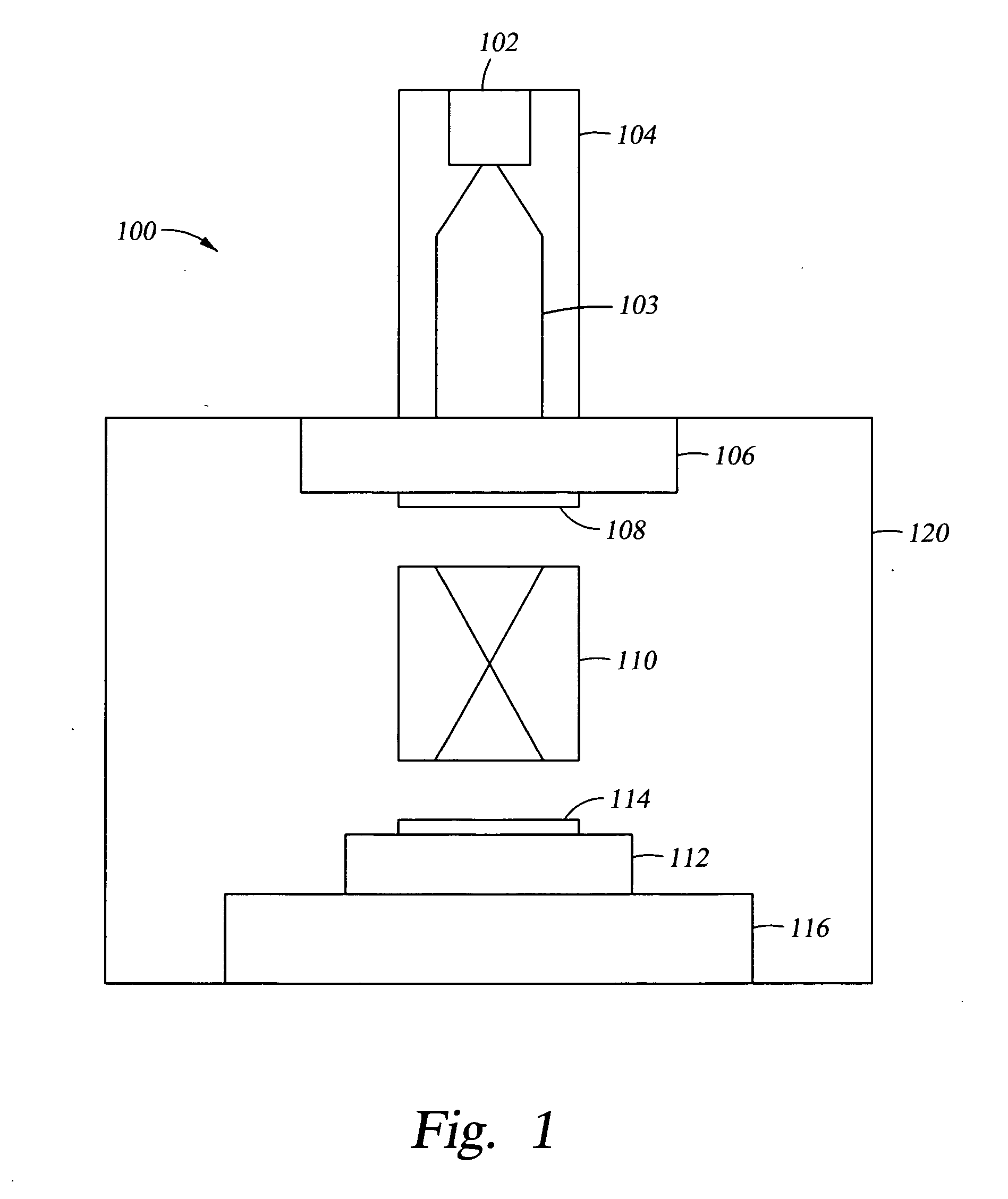
[0021] A system for securely holding a wafer during lithographic processing is described. In the following description, for purposes of explanation, numerous specific details are set forth in order to provide a thorough understanding of the present invention. It will be evident, however, to one of ordinary skill in the art, that the present invention may be practiced without these specific details. The description of preferred embodiments is not intended to limit the scope of the claims appended hereto.

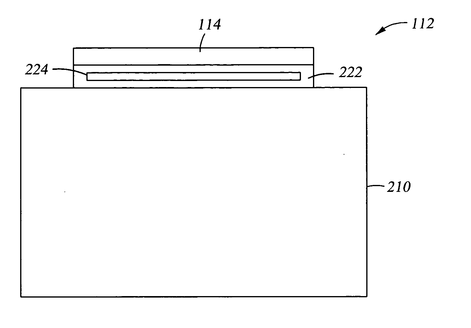
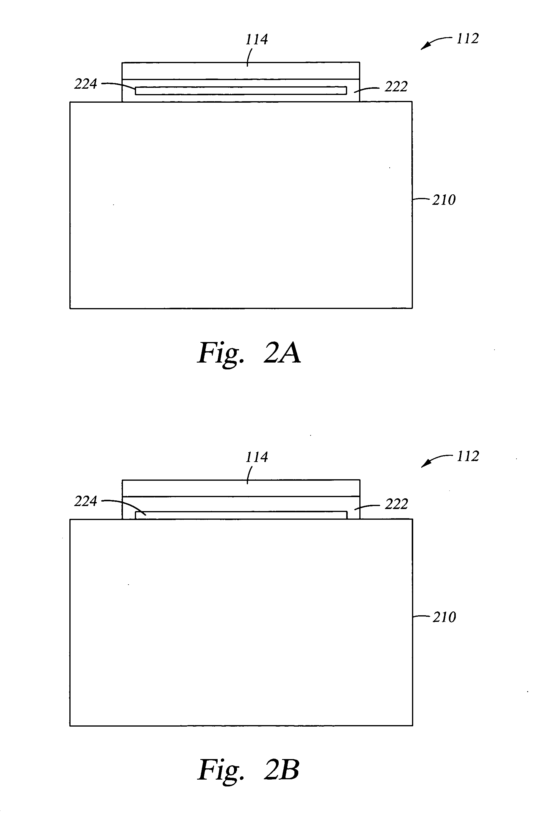
[0022] During lithographic processing, charged particles or radiation are directed through a mask to project an image of portions of the mask onto a substrate, such as a silicon wafer having an energy sensitive or photo resist layer. Typical charged particle beam lithography systems use electron beam or ion beam projection systems to fabricate a wafer using an image mask. In one embodiment of the present invention, the wafer holding system is implemented in a SCALPEL (Scattering with...


PUM


Abstract

A wafer chuck is designed to allow the substrate to thermally deform during charged particle beam lithography. The wafer chuck includes a compliant layer disposed over an chuck body. During lithography processing the wafer is electrostatically held in contact with a flexible compliant layer and the wafer is exposed to the charged particle beam resulting in thermal deformation of the wafer. The compliant layer deforms with the substrate and allows the wafer to deform in a predictable manner.

Description

FIELD OF THE INVENTION [0001] The present invention relates generally to wafer processing systems for semiconductor fabrication, and more specifically to a wafer holder for lithography systems, and other wafer processing steps. BACKGROUND OF THE INVENTION [0002] As the degree of circuit integration has increased, the feature sizes of IC's have dramatically decreased. To support future semiconductor fabrication requirements, lithography systems using charged particle beams, such as electron beams or ion beams, have been developed to overcome feature size limitations of traditional optical systems. In charged particle beam projection lithography systems, portions of a mask are exposed to a charged particle beam to project an image of the mask onto a substrate. Several new charged particle beam lithography systems have been developed to extend lithography capabilities to sub-0.15 micron feature size levels. One such system is a microcolumn electron beam system developed by IBM. This sy...

Claims


Application Information

Patent Timeline
Patent Type & Authority Applications(United States)
IPC IPC(8): H01L21/683H01L21/687
CPCH01L21/68757H01L21/6831
Inventor MOFFATT, STEPHEN
Owner APPLIED MATERIALS INC
Why Eureka
Try Eureka