Word and bit line arrangement for a FinFET semiconductor memory

a technology of semiconductor memory and word and bit line, which is applied in the field of semiconductor memory, to achieve the effect of high storage density of 2f2 per bit, faster access time to each memory cell, and improved scalability

Inactive Publication Date: 2005-09-15
INFINEON TECH AG
View PDF10 Cites 38 Cited by
  • Summary
  • Abstract
  • Description
  • Claims
  • Application Information

AI Technical Summary

Benefits of technology

[0026] The invention thus provides a non-volatile semiconductor memory in a “virtual ground” arrangement (VGA) with a cell array density of 2F2 per bit, in the case of which the bit lines lie in sawtooth-shaped fashion and alternately in the first and second metal planes (bit line planes). This results in a memory arrangement having the storage density of planar NROMs, with the advantage of an adjustable read current, the “double gate” effect by virtue of the FinFET arrangement and thus, a potentially better scalability and also a faster access time to each memory cell by virtue of the metallic bit lines. The very high storage density of 2F2 per bit may also be achieved for fins that are very close together where F<50 nm.

Problems solved by technology

However, charge carriers, for example, electrons in the case of an n-channel FinFET, given suitable source, drain and gate potentials, can acquire such an energy (hot electrons) that they can overcome the fin insulator layer and be permanently trapped by the storage layer.

Method used


Image

  • Word and bit line arrangement for a FinFET semiconductor memory
  • Word and bit line arrangement for a FinFET semiconductor memory
  • Word and bit line arrangement for a FinFET semiconductor memory

Examples


first embodiment

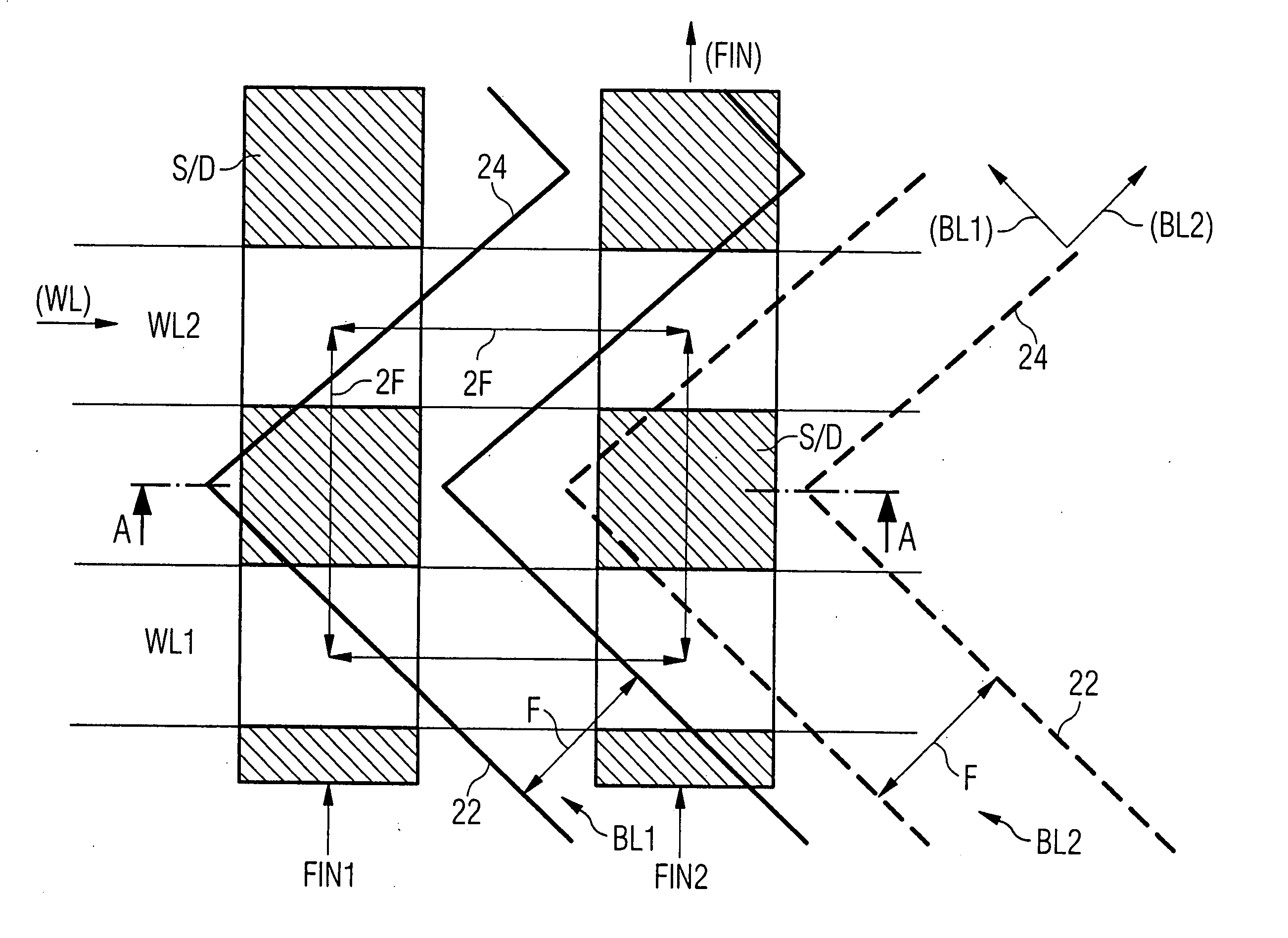
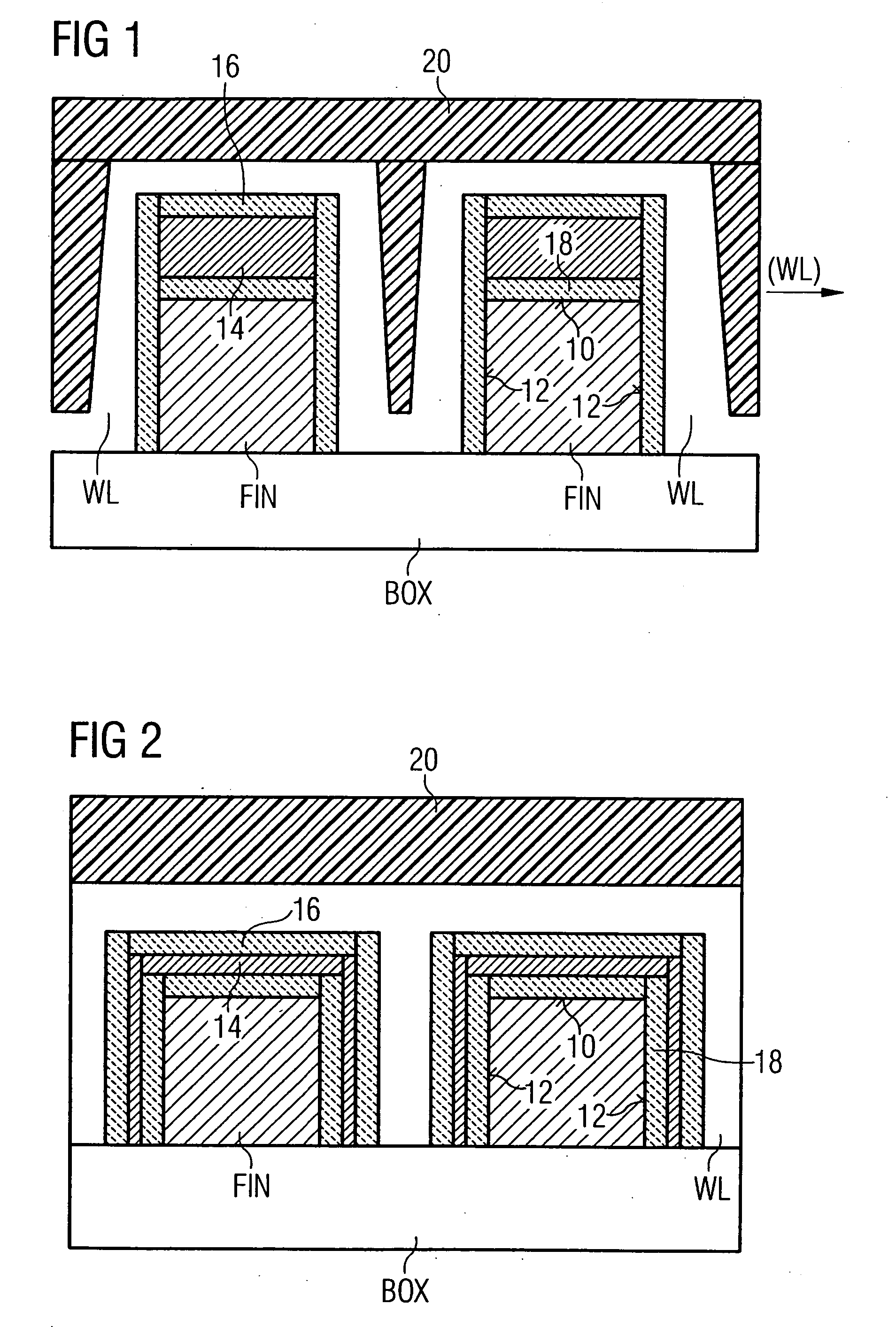
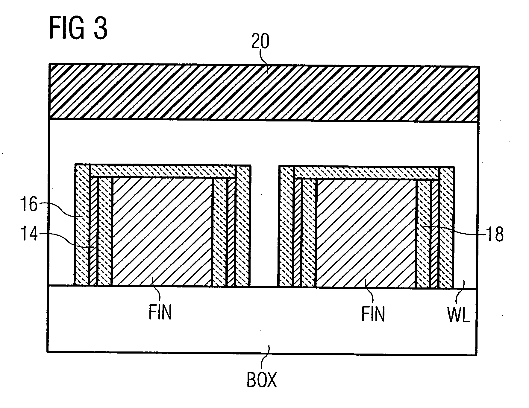
[0041]FIG. 4 shows a simplified plan view of a semiconductor memory according to the invention.

[0042] The ridgelike fins made of semiconductor material FIN1, FIN2 run from top to bottom in the plane of the drawing. The fin longitudinal direction is illustrated by the direction arrow designated by (FIN). In the embodiment illustrated in FIG. 4, fins FIN1, FIN2 have a fin width F corresponding to the minimum structure width of the semiconductor memory. Highly and lightly doped semiconductor sections are provided alternately in the fin longitudinal direction (FIN). The highly doped sections, which are emphasized by a hatched pattern in FIG. 4, form the electrically conductively doped contact regions S / D (source and drain regions of the FinFETs). A channel region in which the FinFET channel is formed is respectively arranged between two contact regions S / D that are adjacent in the fin longitudinal direction (FIN).

[0043] The word lines WL1, WL2 run perpendicular to the fin longitudinal ...

second embodiment

[0048]FIG. 6 shows a semiconductor memory according to the invention in a schematic plan view. Features that have already been described in connection with FIG. 4 bear the same reference symbols and are not described again. In contrast to the embodiment described with reference to FIG. 4, the memory cell array of FIG. 6 only has bit lines BL in a single metal plane (bit line plane). Given a minimum structure width F of the semiconductor memory that corresponds to the width of the bit line BL, it is thus necessary to choose a different dimensioning of the fin width of the fins FIN1, FIN2 and also of the word lines WL1, WL2 and of the word line spacing. Since the bit lines BL run at an angle of 45° to the word line longitudinal direction (WL) and the fin longitudinal direction (FIN), the fin and word line widths and also the word line spacing are F{square root}{square root over (2)}. The memory cell is thus enlarged to a 2F{square root}{square root over (2)}×F{square root}{square root...


PUM


Abstract

The invention relates to a semiconductor memory having a multiplicity of fins made of semiconductor material which are spaced apart from one another, a multiplicity of channel regions and contact regions being formed in each of the fins, a multiplicity of word lines, a multiplicity of storage layers, at least one of the storage layers being arranged between each of the channel regions and the word line, and a multiplicity of bit lines, the longitudinal axes of first bit line portions running parallel to a first bit line direction and the longitudinal axes of second bit line portions running parallel to a second bit line direction, the second bit line direction being rotated relative to the first bit line direction, each of the bit lines being electrically connected to a multiplicity of the contact regions, wherein, between two contact regions of the same fin that are connected to one of the bit lines, a contact region is not connected to the respective bit line.

Description

CROSS-REFERENCE TO RELATED APPLICATIONS [0001] This application is a continuation of co-pending PCT patent application No. PCT / EP03 / 09294, filed 21 Aug. 2003, which claims the benefit of German patent application serial number DE 102 41 171.9, filed 5 Sep. 2002. Each of the aforementioned related patent applications is herein incorporated by reference in their entireties.BACKGROUND OF THE INVENTION [0002] 1. Field of the Invention [0003] The invention relates to a semiconductor memory, and more particularly, to a semiconductor memory having FinFET elements. [0004] 2. Description of the Related Art [0005] Conventional non-volatile semiconductor memory elements exist in a multiplicity of different embodiments, e.g., PROM, EEPROM, FLASH EEPROM and SONOS, depending on the application. These various embodiments differ in particular in terms of erasure option, programmability and programming time, retention time, storage density and also in terms of their production costs. There is a part...

Claims


Application Information

Patent Timeline
Patent Type & Authority Applications(United States)
IPC IPC(8): H01L21/8247H01L21/336H01L21/8246H01L27/105H01L27/115H01L29/788H01L29/792
CPCH01L27/115H01L27/11568H01L29/792H01L29/785H01L29/66833H10B43/30H10B69/00
Inventor HOFMANN, FRANZSCHULZ, THOMASSPECHT, MICHAEL
Owner INFINEON TECH AG
Why Eureka
Try Eureka