System for reducing the electrical return loss of a lithium niobate traveling wave optical modulator with low characteristic impedance

a traveling wave optical modulator and characteristic impedance technology, applied in the field of fiber optics, can solve the problems of overall worsening performance, reducing the gap width between hot and ground electrodes of coplanar transmission lines, and overall worsening performance, so as to reduce driving voltage design, reduce chip length, and reduce the effect of electrical return loss

Active Publication Date: 2005-09-15
OCLARO NORTH AMERICA
View PDF11 Cites 15 Cited by
  • Summary
  • Abstract
  • Description
  • Claims
  • Application Information

AI Technical Summary

Benefits of technology

[0007] The present invention overcomes the foregoing problems by providing an electro-optical modulator that has a microwave thin film resistor (or a lumped resistor) on an accessory connection chip located between the RF connector of the microwave input and the RF electrode of the Lithium Niobate chip. The accessory connection chip has a broadband attenuator, such as a thin film resistor, which is placed in a microstrip line to ensure that the electrical transmission reaches the Lithium Niobate chip. The insertion of the thin film resistor before the RF electrode lowers the electrical return loss, allowing a lower driving voltage design or a reduced chip length.

Problems solved by technology

Conventional solutions employ three design techniques for reducing a RF driving voltage in a Lithium Niobate (“LN”) travelling wave modulator: (1) adopting a longer RF electrode, and thus resulting in a longer, instead of a shorter, chip; (2) decreasing the buffer-layer thickness, resulting in an overall worsening of the performances; and (3) decreasing the gap width between hot and ground electrodes of the CoPlanar transmission line, resulting once more in an overall worsening of the performances.
In addition, the total electrical losses increase, thereby decreasing the electro-optical bandwidth.
Thus, such a solution is not suitable for designing metro application-oriented components.
Second, if the buffer-layer thickness is decreased, the electro-optical bandwidth also decreases due to the total electrical losses increasing and microwave effective refractive index being more difficult to be matched to the optic.
Furthermore, the characteristic impedance of the microwave lines becomes worse, rendering more difficult to have a good electrical return loss vs. frequency profile.
Third, if the gap width is decreased between hot and ground electrodes of the CoPlanar transmission line, the electro-optical bandwidth decreases due to the increasing in total electrical losses, while the characteristic impedance of the microwave lines becomes worse.

Method used


Image

  • System for reducing the electrical return loss of a lithium niobate traveling wave optical modulator with low characteristic impedance
  • System for reducing the electrical return loss of a lithium niobate traveling wave optical modulator with low characteristic impedance
  • System for reducing the electrical return loss of a lithium niobate traveling wave optical modulator with low characteristic impedance

Examples


Embodiment Construction

)

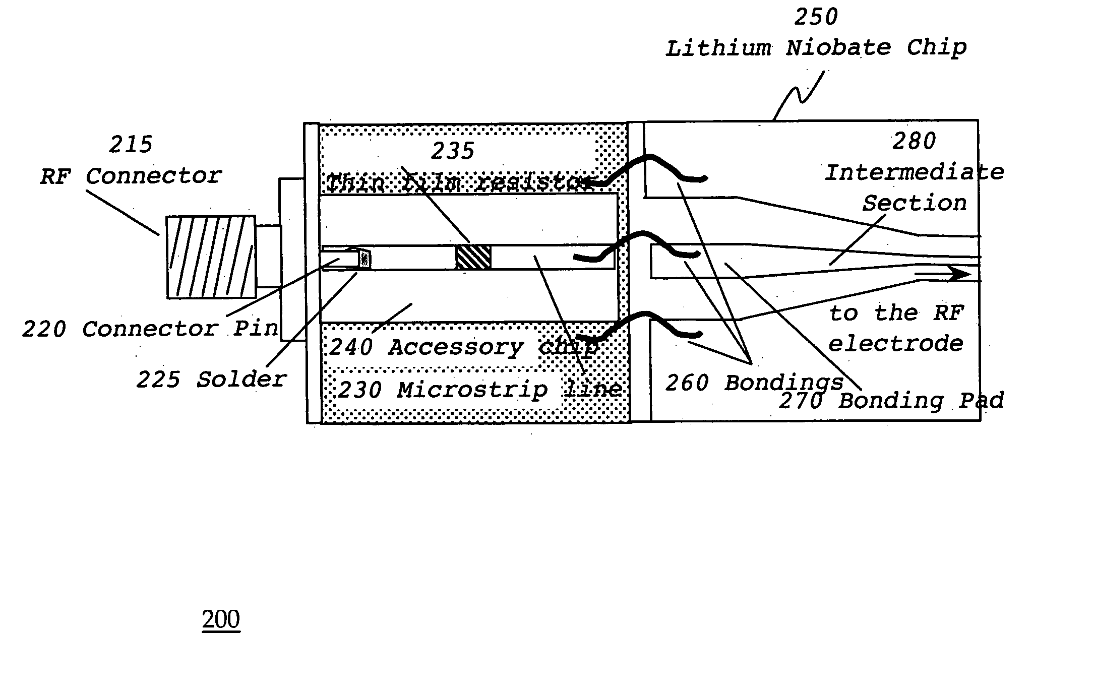
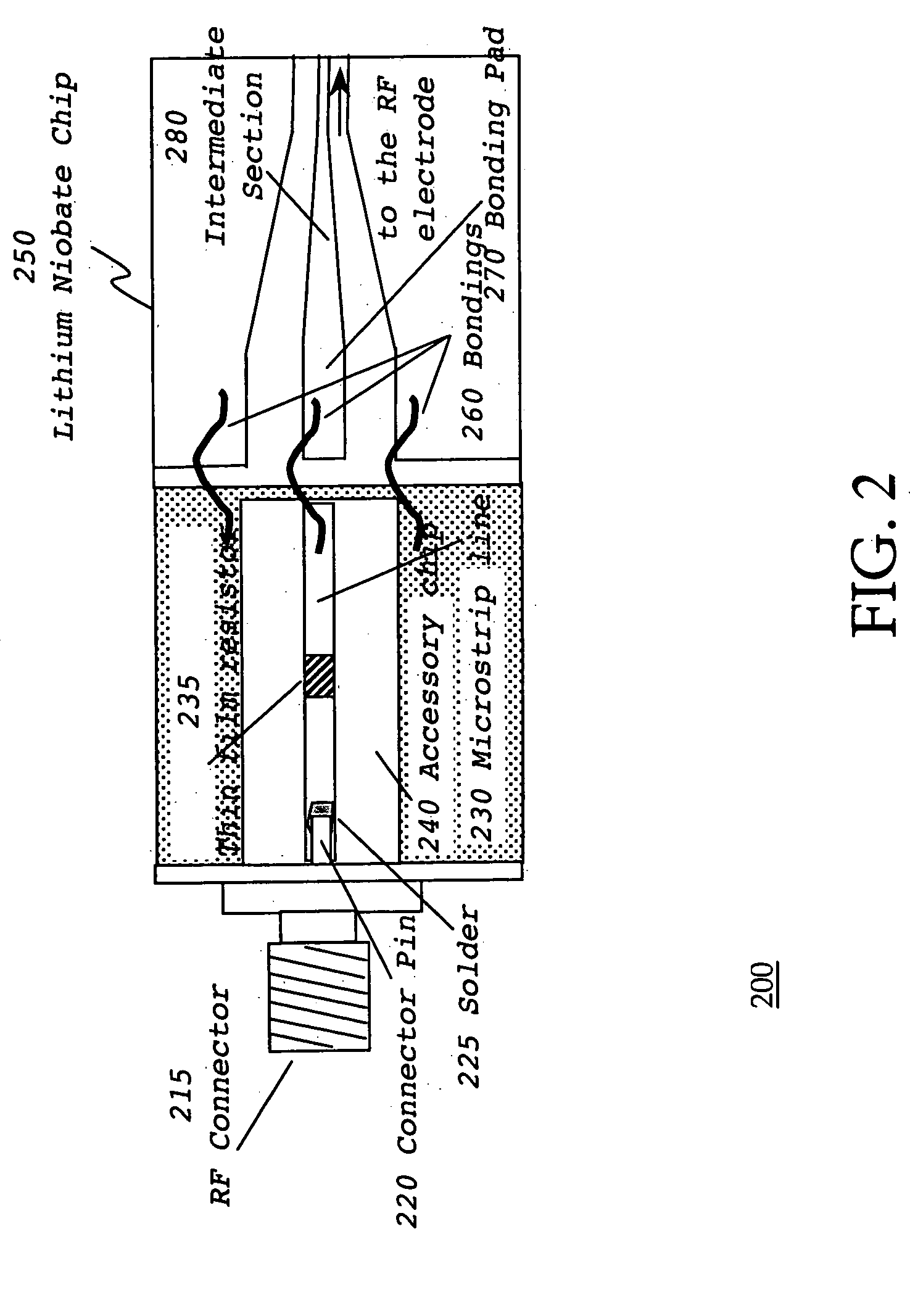
[0016] Referring now to FIG. 2, there is shown a structural diagram illustrating an electro-optical modulator 200 with a RF electrical circuit employing a thin resistive film in accordance with the present invention. The electro-optical modulator 200 comprises a microwave input chip or an accessory chip 240, which is coupled to the Lithium Niobate chip 250 through one or more wire bondings 260, ribbons, soldering, or dots of resin. In order to ease bonding adhesion, one or more of bonding pads 270 are placed on the Lithium Niobate chip 250, with a tapered impedance-controlled structure connecting the one or more bonding pads 270 to the modulating RF line positioned near the optical waveguides.

[0017] The accessory chip 240 has a broadband attenuator, such as a thin film resistor 235, for connecting a RF connector 215 to a RF line or an intermediate section to the RF electrode 280 of the Lithium Niobate chip 250. A microwave path in the microstrip line 230 could be interrupted in a ...


PUM

PropertyMeasurementUnit
impedanceaaaaaaaaaa
impedanceaaaaaaaaaa
impedanceaaaaaaaaaa

Abstract

An electro-optical modulator is disclosed that has a microwave input, chip with a thin film resistor or a lumped resistor located between an input RF connector and an RF electrode on a Lithium Niobate chip. The accessory connection chip has a broadband attenuator like a thin film resistor which is placed in a microstrip line for effecting the electrical transmission to Lithium Niobate chip. The insertion of the thin film resistor before the RF electrode lowers the electrical return loss value as a function of frequency, allowing a lower driving voltage design or a reduced chip length without degrading the performances.

Description

BACKGROUND INFORMATION [0001] 1. Technical Field of the Invention [0002] The invention relates generally to the field of fiber optics and more particularly to electro-optical modulators. [0003] 2. Description of Related Art [0004] Electro-optical modulators in a recent trend are moving toward conjugating smaller dimensions and lower driving voltages to enable system vendors to design their opto-electronic boards, e.g. transponders, by adopting smaller footprints, with inexpensive and low power electronic components. Conventional solutions employ three design techniques for reducing a RF driving voltage in a Lithium Niobate (“LN”) travelling wave modulator: (1) adopting a longer RF electrode, and thus resulting in a longer, instead of a shorter, chip; (2) decreasing the buffer-layer thickness, resulting in an overall worsening of the performances; and (3) decreasing the gap width between hot and ground electrodes of the CoPlanar transmission line, resulting once more in an overall wo...

Claims


Application Information

Patent Timeline
Patent Type & Authority Applications(United States)
IPC IPC(8): G02F1/03G02F1/035
CPCG02F1/0121G02F1/0356G02F1/225G02F1/0327
Inventor GILARDI, GIOVANNIMILANESE, PAOLOPENSA, SIMONEBONAZZOLI, MARIOGOBBI, LUIGI
Owner OCLARO NORTH AMERICA
Why Eureka
Try Eureka