Locally thinned fins

a technology of local thinning and fins, applied in the direction of transistors, electrical devices, semiconductor devices, etc., can solve the problems of reducing the ability of the gate to control whether the device is placed or not, degrading the ability of the gate to control whether the device is placed, and achieving the effect of reducing the thickness

Active Publication Date: 2005-09-15
IBM CORP
View PDF13 Cites 34 Cited by
  • Summary
  • Abstract
  • Description
  • Claims
  • Application Information

AI Technical Summary

Benefits of technology

[0018] The present invention is directed to a process for fabricating FinFET transistor structures, in which the fins in the transistor body area are decreased in thickness compared with the fins in the S / D areas.

Problems solved by technology

As MOSFETs are scaled to channel lengths below 100 nm, conventional MOSFETs suffer from several problems.
In particular, interactions between the source and drain of the MOSFET degrade the ability of the gate to control whether the device is on or off.
As device size is scaled, however, this becomes increasingly difficult, since the distance between the source and drain is reduced, and hence, they increasingly interact with the channel, reducing gate control and increasing short channel effects (SCE).
As the dimensions of structures or features on the integrated circuit reach levels below 100 nm or 50 nm, lithographic techniques are unable to precisely and accurately define the feature.
However, patterning narrow, dense active regions is challenging.
As discussed above with respect to gate conductors, conventional lithographic tools are unable to accurately and precisely define active regions as structures or features with dimensions below 100 nm or 50 nm.

Method used


Image

  • Locally thinned fins
  • Locally thinned fins
  • Locally thinned fins

Examples


Embodiment Construction

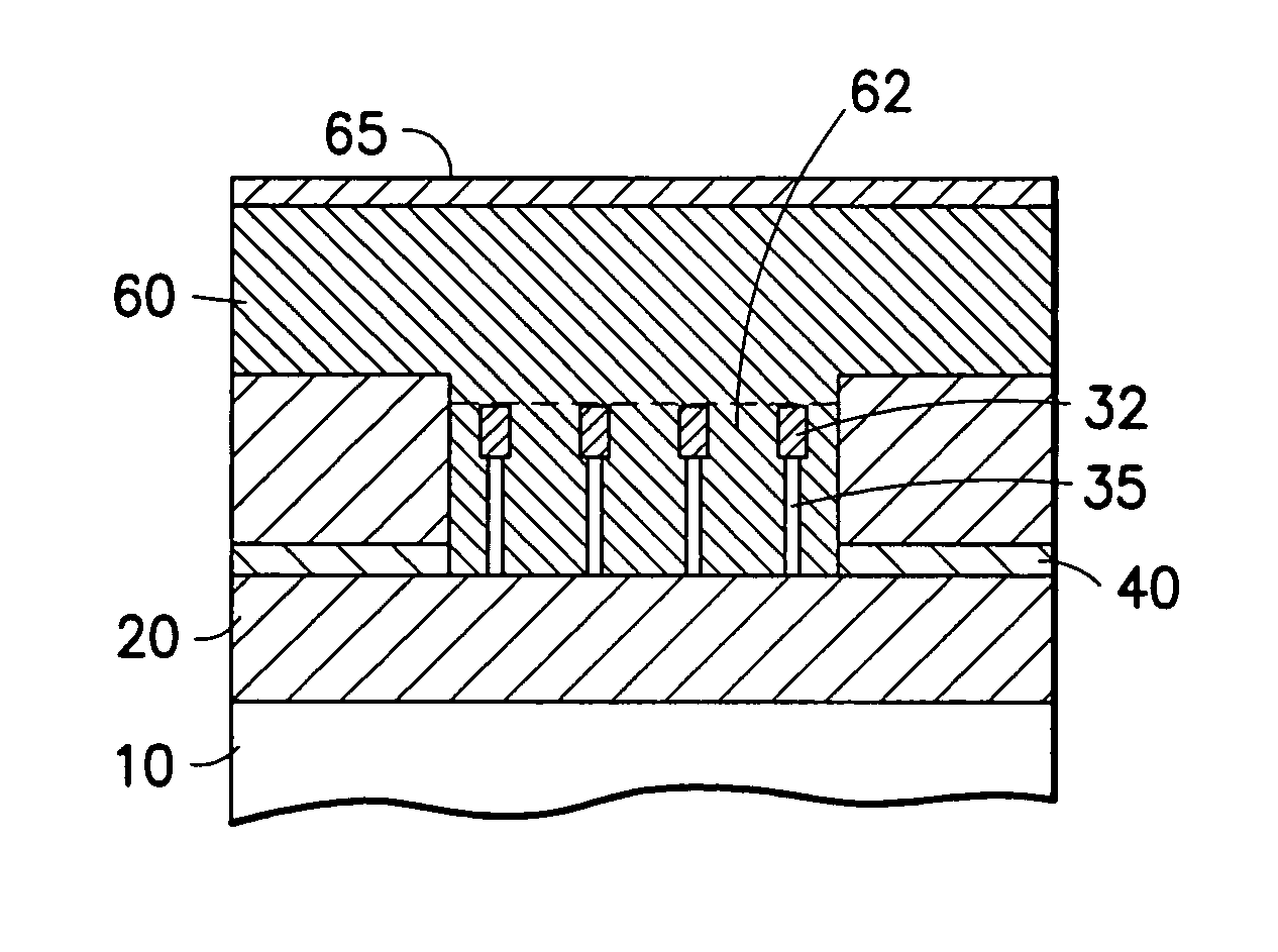
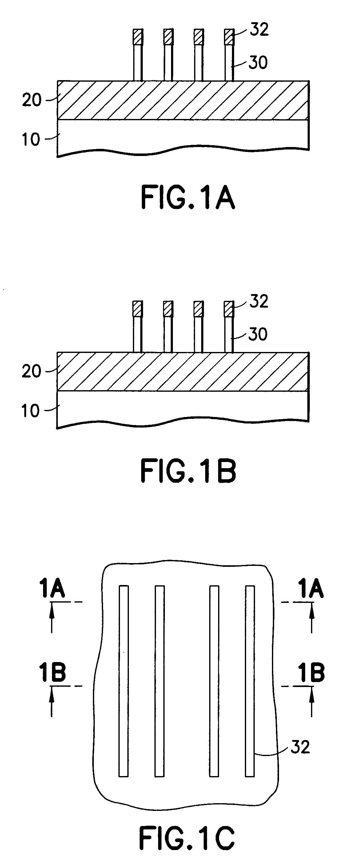
[0032] This invention describes a process to fabricate locally thinned fins in the body region of the transistor. The advantage of a locally thinned fin is: Higher mechanical stability of thin fins (since most of the fin is thicker and stronger than the thin region); formation of halos and extension by ion implant; and because due to the thicker fin body outside the gate not all of the silicon is amorphized and amorphized silicon can therefore be recrystallized again.

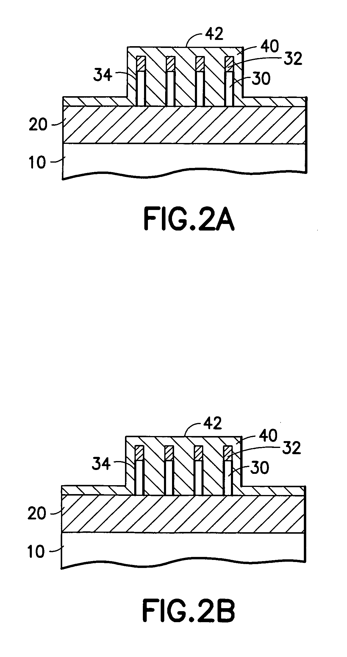
[0033] A feature of the invention is a gate spacer process that protects the gate while the sidewall of the fins is cleared from the gate spacer material (e.g. nitride) and from other materials. Clearing the fin sidewall from unwanted spacer material is quite difficult as a long overetch of the gate spacer is required. This overetch that clears the sidewall of the fins also consumes the conformal gate spacer on top and on the upper sides of the gate, thereby exposing the polysilicon gate material. Cleared fin sidewalls...


PUM


Abstract

In a FinFET integrated circuit, the fins are formed with a reduced body thickness in the body area and then thickened in the S/D area outside the body to improve conductivity. The thickening is performed with epitaxial deposition while the lower portion of the gates are covered by a gate cover layer to prevent thickening of the gates at the fin level, which may short the gate to the S/D.

Description

TECHNICAL FIELD [0001] The field of the invention is that of fabricating field effect transistors having a body extending perpendicular to the semiconductor substrate between horizontally disposed source and drain regions, referred to as a “FinFET”. BACKGROUND OF THE INVENTION [0002] Metal-Oxide-Semiconductor field effect transistor (MOSFET) technology is the dominant electronic device technology in use today. Performance enhancement between generations of devices is generally achieved by reducing the size of the device, resulting in an enhancement in device speed. This is generally referred to as device “scaling”. [0003] Ultra-large-scale integrated (ULSI) circuits generally include a multitude of transistors, such as more than one million transistors and even several million transistors that cooperate to perform various functions for an electronic component. The transistors are generally complementary metal oxide semiconductor field effect transistors (CMOSFETs) which include a ga...

Claims


Application Information

Patent Timeline
Patent Type & Authority Applications(United States)
IPC IPC(8): H01L21/28H01L21/00H01L21/335H01L21/336H01L29/41H01L29/423H01L29/49H01L29/772H01L29/78H01L29/786
CPCH01L29/785H01L29/66818
Inventor BEINTNER, JACHEN C.
Owner IBM CORP
Why Eureka
Try Eureka