High density plasma process for silicon thin films

Inactive Publication Date: 2005-09-15
SHARP KK
View PDF5 Cites 27 Cited by
  • Summary
  • Abstract
  • Description
  • Claims
  • Application Information

AI Technical Summary

Benefits of technology

[0016] The present invention describes a novel deposition method for the fabrication of Si thin films by high-density plasma-based processes, employing an inductively coupled plasma source. The high-density plasma processes generate high electron/ion concentrations, with suitable electron temperatures, to enhance the deposition of Si. The high-density plasma process is characterized by high elect

Problems solved by technology

The carrier mobility of transistors fabricated with a-Si is poor, insufficient for LCD driver circuits.
Impurity contamination can severely degrade the device performance.
However, as mentioned above, there are also dis

Method used


Image

  • High density plasma process for silicon thin films
  • High density plasma process for silicon thin films
  • High density plasma process for silicon thin films

Examples


Embodiment Construction

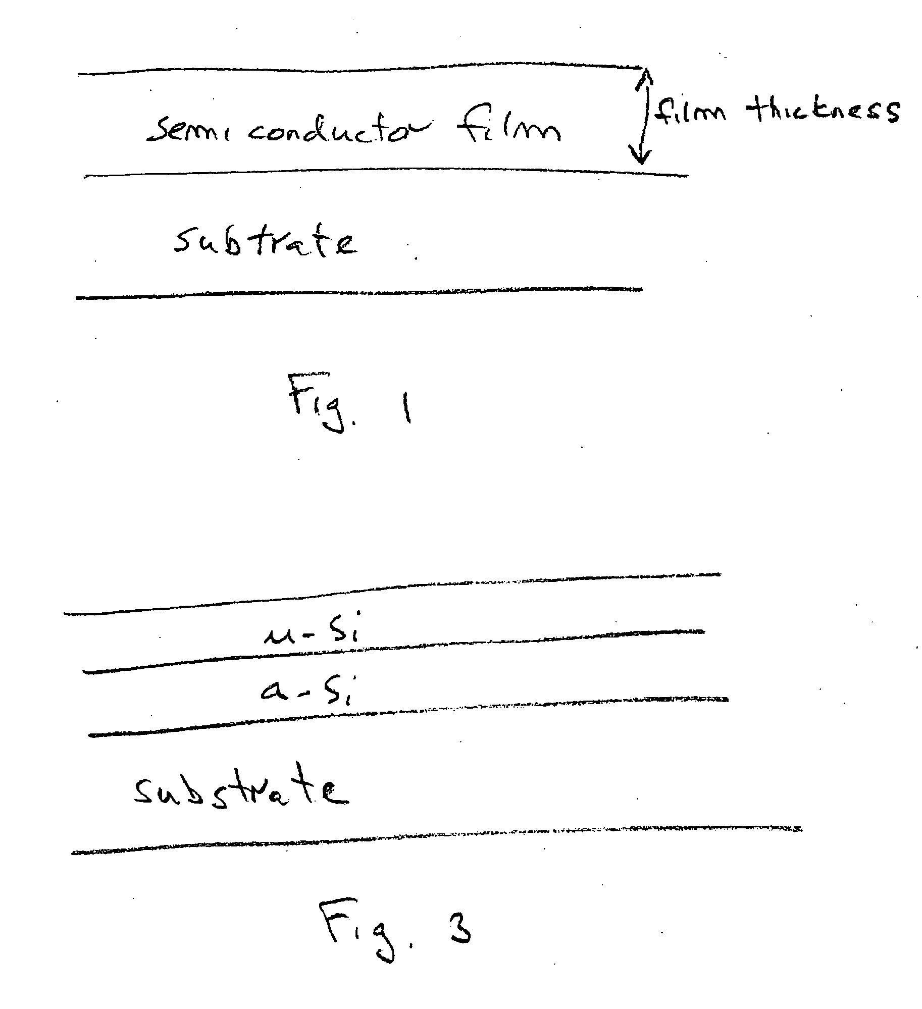
[0026]FIG. 1 is a partial cross-sectional view of the semiconductor film formed using the present invention low temperature, HD plasma deposition process.

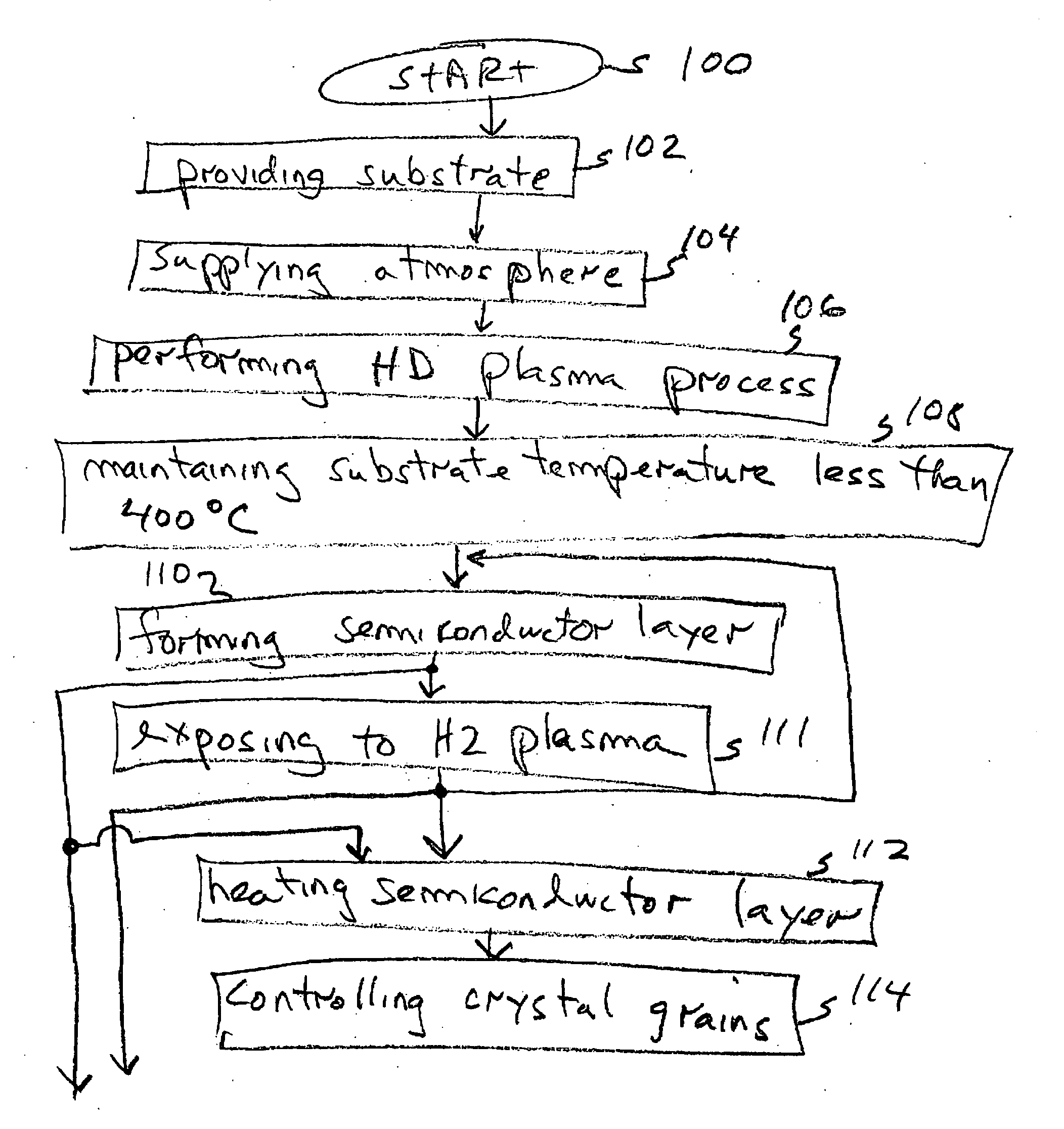
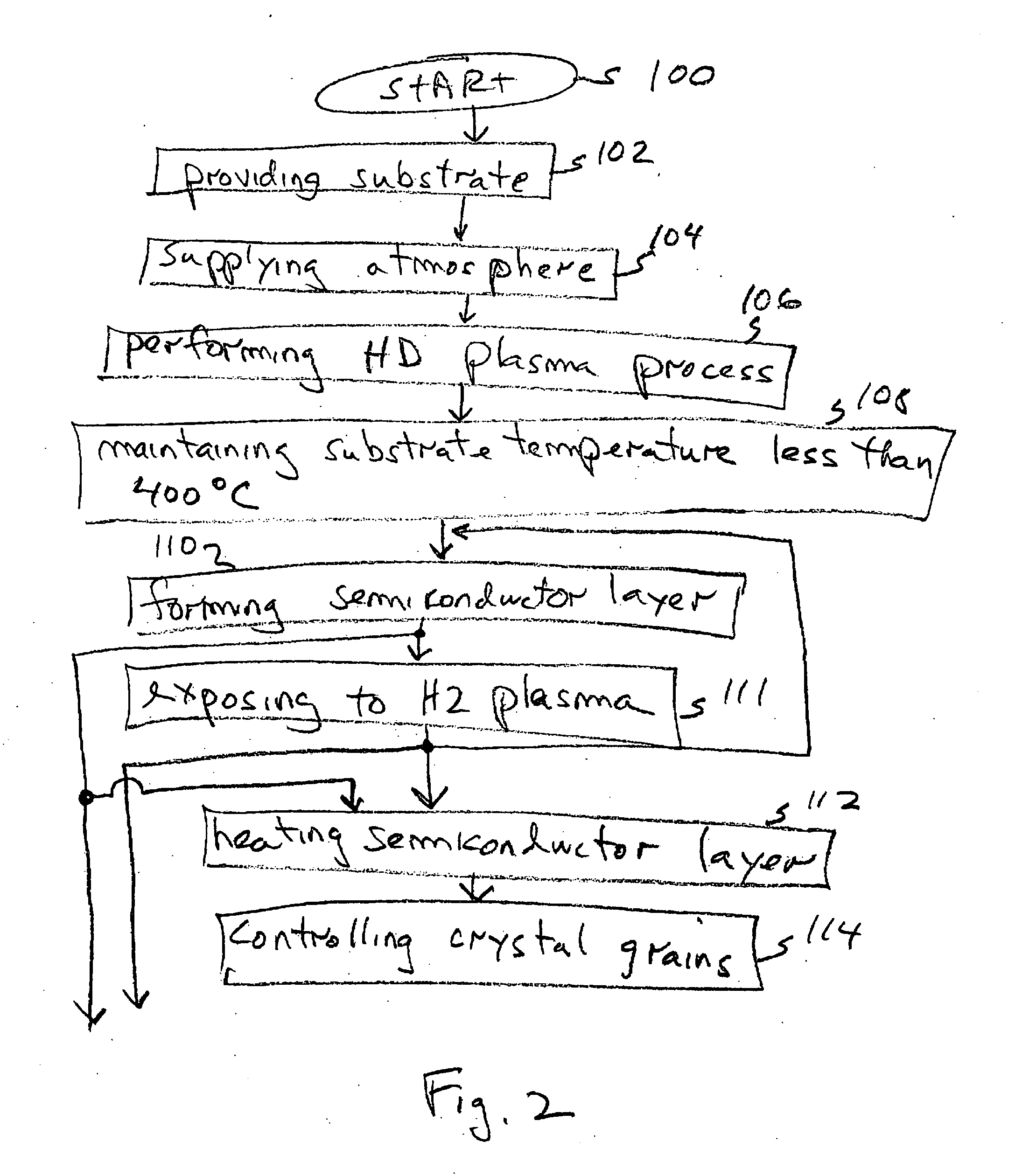
[0027]FIG. 2 is a flowchart illustrating the present invention method forming a semiconductor thin film. Although the method is depicted as a sequence of numbered steps for clarity, no order should be inferred from the numbering unless explicitly stated. It should be understood that some of these steps may be skipped, performed in parallel, or performed without the requirement of maintaining a strict order of sequence. The method starts at Step 100.

[0028] Step 102 provides a substrate. Although the invention is not necessarily so limited, it is especially advantageous for use with low-temperature glass or plastic substrates, as might be used LCD fabrication. Step 104 supplies an atmosphere. Step 106 performs a high-density (HD) plasma process. Step 108 maintains a substrate temperature of 400 degrees C., or less. Again, the proce...


PUM

PropertyMeasurementUnit
Thicknessaaaaaaaaaa
Pressureaaaaaaaaaa
Fractionaaaaaaaaaa

Abstract

A method is provided for forming a Si and Si—Ge thin films. The method comprises: providing a low temperature substrate material of plastic or glass; supplying an atmosphere; performing a high-density (HD) plasma process, such as an HD PECVD process using an inductively coupled plasma (ICP) source; maintaining a substrate temperature of 400 degrees C., or less; and, forming a semiconductor layer overlying the substrate that is made from Si or Si-germanium. The HD PECVD process is capable of depositing Si at a rate of greater than 100 Å per minute. The substrate temperature can be as low as 50 degrees C. Microcrystalline Si, a-Si, or a polycrystalline Si layer can be formed over the substrate. Further, the deposited Si can be either intrinsic or doped. Typically, the supplied atmosphere includes Si and H. For example, an atmosphere can be supplied including SiH4 and H2, or comprising H2 and Silane with H2/Silane ratio in the range of 0-100.

Description

RELATED APPLICATIONS [0001] This application is a continuation-in-part of a pending patent application entitled, METHODS FOR FABRICATING OXIDE THIN FILMS, invented by Joshi et al., Ser. No. 10 / 801,374, filed Mar. 15, 2004. [0002] This application is a continuation-in-part of a pending patent application entitled, DEPOSITION OXIDE WITH IMPROVED OXYGEN BONDING, invented by Pooran Joshi, Ser. No. 10 / 801,377, filed Mar. 15, 2004. [0003] This application is a continuation-in-part of a pending patent application entitled, HIGH DENSITY PLASMA PROCESS FOR THE FORMATION OF SILICON DIOXIDE ON SILICON CARBIDE SUBSTRATES, invented by Joshi et al., Ser. No. 10 / 812,591, filed Mar. 29, 2004.BACKGROUND OF THE INVENTION [0004] 1. Field of the Invention [0005] This invention generally relates to integrated circuit (IC) fabrication and, more particularly, to a system and method for forming silicon-containing films at low process temperatures using a high density plasma source. [0006] 2. Description of...

Claims


Application Information

Patent Timeline
IPC IPC(8): H01L29/872B05D5/12C23C16/24C23C16/455C23C16/509C30B1/00H01L21/00H01L21/04H01L21/20H01L21/205H01L21/31H01L21/316H01L21/36H01L21/42H01L21/469H01L29/47H01L29/786
CPCC23C16/24C23C16/45523C23C16/509H01L21/049H01L21/0262H01L21/02422H01L21/0245H01L21/02532H01L21/31612H01L21/02164
Inventor JOSHI, POORAN CHANDRAVOUTSAS, APOSTOLOS T.HARTZELL, JOHN W.
Owner SHARP KK
Why Eureka
Try Eureka