Three-dimentional components prepared by thick film technology and method of producing thereof

a technology of three-dimensional components and thick film, applied in the direction of positive displacement liquid engines, optical light guides, screen printers, etc., can solve the problems of high technological requirements, difficult production of more complicated structures, and inability to integrate complex chemical processes

Inactive Publication Date: 2005-09-22
ING ILJA KREJCI ENG
View PDF2 Cites 122 Cited by
  • Summary
  • Abstract
  • Description
  • Claims
  • Application Information

AI Technical Summary

Problems solved by technology

The main disadvantage of all these chemical sensors is that there is no possibility to integrate complicated chemical processes.
The disadvantage of the first example is the high technological requirements and difficult production of more complicated structures.
The disadvantage of the second one is the low reliability of the sticked parts and the inflow of the glue into the sensor's active structure.
Their common disadvantage is their demanding large-scale production and in many cases their price.
The disadvantage of known methods e.g. micro-cut needs a long time of preparation and the necessity of expensive machines, etching is time consuming and the technology is expensive, laser-cut is very expensive and the monolithic technology is a very costly technology.
The geometrical limits are too low for the application in microsensors with fluidic circuits.

Method used


Image

  • Three-dimentional components prepared by thick film technology and method of producing thereof
  • Three-dimentional components prepared by thick film technology and method of producing thereof
  • Three-dimentional components prepared by thick film technology and method of producing thereof

Examples


example 1

Flow Through Filter Produced by Thick Film Technology

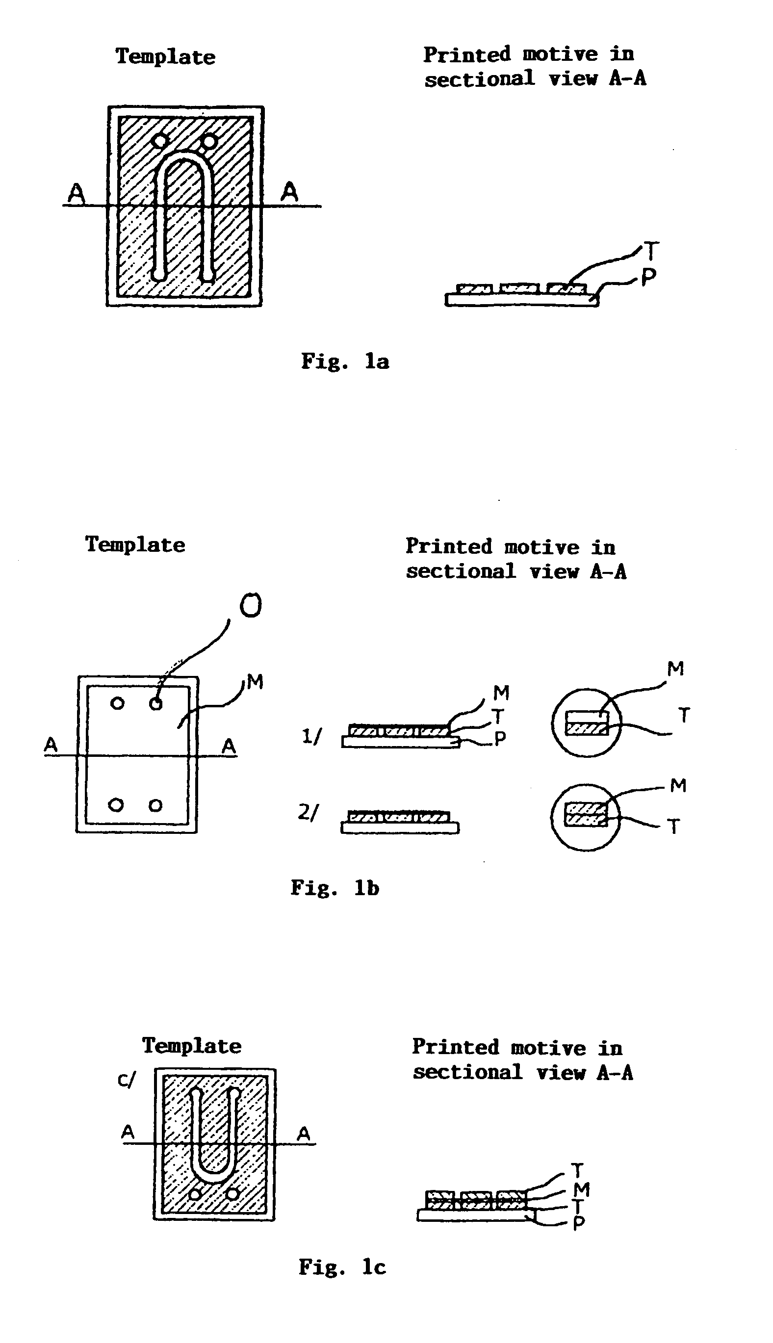
[0042] The flow through filter production steps are described in FIGS. 1a to 1y. Layer T that create the channel for filtered liquid input and a collecting channel for a filtrate output is printed on a ceramic pad P in the first step (FIG. 1a). There is used e.g. a polymer paste Du Pont 5483. The width of the channel is 250 μm, its height is 15 μm.

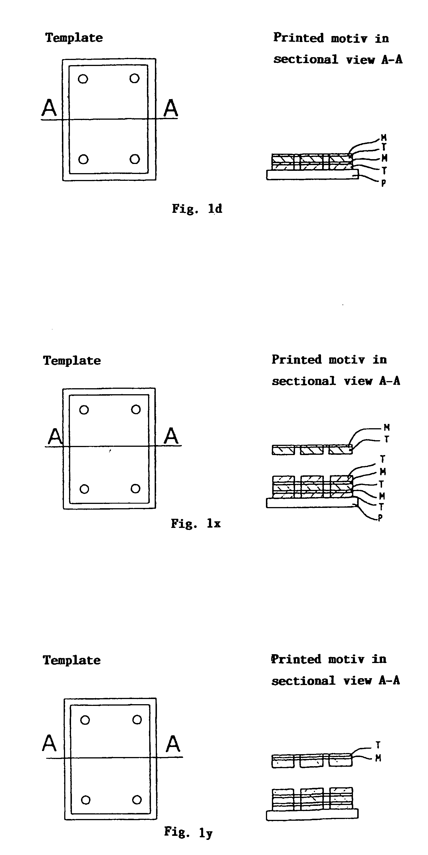
[0043] On the non-hardened print of the previous layer is put a porous membrane M produced from polyethylene terephthalate neucleopor with 1 μm pores and a thickness of 10 μm (see FIG. 1b-1). The membrane has four holes O for liquid inflow and filtrate output. Owing to a surface tension is the paste partly sucked in the membrane at the contact sites between the membrane and paste (FIG. 1b-2) and a homogenous connection with the printed layer T occurs. The channel is closed and the pores stay free.

[0044] In the third step (FIG. 1c) the channel for filtrate output and channels for liqu...

example 2

Capillary Electrophoresis with Conductivity Detection

[0049] The production technique is shown in FIGS. 3a to 3f. Basic conducting links motive are printed on a corundum pad P in the first step using for example Ag conducting paste Tesla 9220 (FIG. 3a). The electrodes for electrophoresis and conducting detector electrodes E are printed in the next step using for example Au paste Du Pont 4140. The substrate is fired at 850° C. and the basic electric net formed. The channel structure 5 is printed using a dielectric paste (Du Pont 5483, for example) in the step figured in FIG. 3c. The appropriate channel side walls height is achieved by repeating this step. The membrane from polyethylene terephthalate nucleopor with 1 μm pores and thickness of 20 μm is inserted in the step figured in FIG. 3d and it is provided with holes O. The production is finished by printing the upper covering layer (FIG. 3e). Whole system is cured at 200° C. for 20 minutes. The entry part for easier sample applyi...

example 3

Microdialyzing Unit with a Biosensor

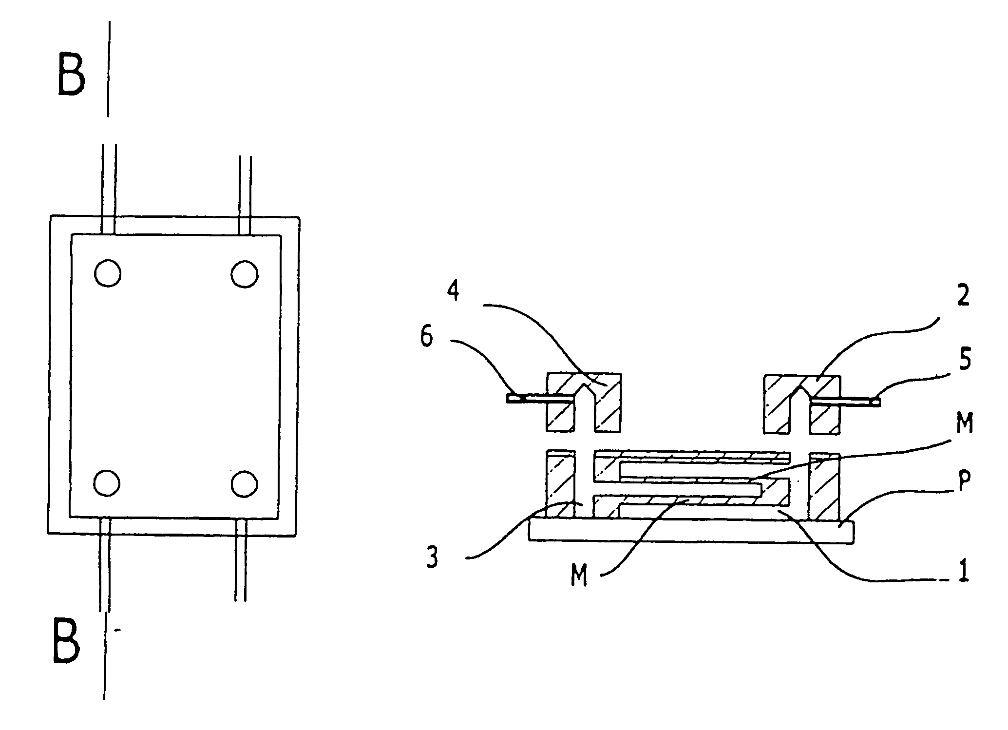
[0052] The production process according to the invention can be used with advantage for construction of microdialyzing unit for continual blood analyzis by biosensor. The schema of the unit is on the FIG. 4. Directly to the injection needle is integrated a miniature system of the size 25×7 mm, which contains three electrode amperometric biosensor and dialyzing cell, which allows the separation of plasma from the blood and its dilution. Blood is inputting to the sensor by injection needle 1 inserted to the patient's vein. Than it runs through the channel created in the way according to the invention, whereby from point 9 till point 8 the channel bottom is formed by a half penetrating membrane. Blood is lead away by mouth piece 2. Dialyzing liquid enters at point 3 and is lead through the channel, the ceiling of which is in the part signed 8 and 2 common for the channel bottom for blood. This is a point where dialysis of low molecular weight speci...


PUM

PropertyMeasurementUnit
thicknessaaaaaaaaaa
sizeaaaaaaaaaa
thicknessaaaaaaaaaa

Abstract

Object of the present invention are components with three dimensional structure prepared by thick film technology by print, where between the printed layers is inserted at least one membrane. The membrane is according to the present to invention at least in a part of the final product. The membrane can be provided with holes which are necessary for next technological steps. The inserted membranes can have pores of the size of 50˜tm to 10 nm and a thickness of 1 to 200˜tm. Method of producing of components with three-dimensional structure by thick film printing technology according to the invention lies in that between some of the printed layers is inserted a suitable membrane, which allows to lay on next layers without influence to previous layers. The printing can be done by screen-printing.

Description

TECHNICAL FIELD [0001] The invention relates to three-dimensional components prepared by thick film technology and method of preparing thereof. BACKGROUND ART [0002] The thick film technology is a technology of creating two dimensional structures by printing followed by curing. The most used type of printing is the screen-printing. Plug printing and jet-printing are also rarely used. Hardening is usually carried out by firing which removes volatile components that provide good technological properties of printing. Hardening of layers is possible by drying at normal or slightly higher (60-150° C.) temperature when using polymer pastes. [0003] Thick film technology is most of all used in electronics for special electronic circuits production. Conducting nets, resistors and capacitors are produced by paste printing on a corundum pad. The pastes contain a base organic part and active metal or dielectric material. [0004] The decomposition of organic matrix and bond of active component on...

Claims


Application Information

Patent Timeline
Patent Type & Authority Applications(United States)
IPC IPC(8): B01D61/18B01D61/28G01N27/07B01D63/08B01L3/00B81B1/00B81C1/00F04B43/04G01F1/684G01N27/30G01N27/327G01N27/403G01N27/447
CPCB01D61/18B01D63/088B01D63/081B01L3/502707B01L2300/0645B01L2300/0681B01L2300/0816B01L2300/0874B01L2300/0887B01L2400/0418B01L2400/0421B81B2201/0264B81B2203/0127B81C1/0046B81C2201/019F04B43/043G01F1/6845G01N27/4473G01N27/44791B01D61/28
Inventor KREJCI, JAN
Owner ING ILJA KREJCI ENG
Why Eureka
Try Eureka