
Photoelectric conversion element and method of manufacturing the

a technology of photoelectric conversion element and manufacturing method, which is applied in the direction of basic electric elements, transistors, solid-state devices, etc., can solve the problems of unavailing increase light intensity, decrease in light impinging on the photoelectric conversion element, and not quite suited to a photoelectric conversion element, so as to prevent the increase in the number of defects on the surface of the substra

Inactive Publication Date: 2005-09-22
TOYOTA JIDOSHA KK
View PDF9 Cites 19 Cited by
  • Summary
  • Abstract
  • Description
  • Claims
  • Application Information

AI Technical Summary

Benefits of technology

The invention provides a photoelectric conversion element and a method of manufacturing it that can reduce carrier recombination loss and increase conversion efficiency. The element has electrodes and semiconductor layers for collecting carriers only on the back surface of a semiconductor substrate, and includes a semiconductor thin film or insulative film with elements that cause conductivity identical or different to the substrate. Diffusion layers are formed on the substrate through diffusion of the elements in the thin film, with one layer containing a higher concentration of the element and forming a pn junction with the substrate. The method includes depositing the thin film or insulative film on the substrate using plasma CVD or MOCVD methods, with high precision and prevention of surface defects. The technical effects include reducing carrier recombination loss, increasing conversion efficiency, and improving the performance of TPV power generation systems.

Problems solved by technology

Because Si (silicon) as a generally employed material can convert only light beams having a wavelength equal to or smaller than 1.1 μm into electricity, it is not quite suited for a photoelectric conversion element.
However, if the area of the front surface side electrode increases, the amount of light impinging on the photoelectric conversion element decreases, whereby a drawback, that is, unavailingness of an increased light intensity is caused.
However, if a thermal diffusion method or an ion implantation method applied to a Si material is used as a method of forming the diffusion layer, the following problems are caused.
Thus, the number of crystal defects on the surface increases, and the recombination loss increases.
Hence, if the ion implantation method is applied to the light-receiving surface side where a large number of carriers are generated, there arises an obstacle to the enhancement of the photoelectric conversion efficiency.
Thus, the Ge surface is inhomogeneously oxidized and becomes rough, whereby the number of crystal defects is increased.
Accordingly, in this case as well, there arises an obstacle to the enhancement of the photoelectric conversion efficiency.

Method used


Image

  • Photoelectric conversion element and method of manufacturing the
  • Photoelectric conversion element and method of manufacturing the
  • Photoelectric conversion element and method of manufacturing the

Examples


first embodiment

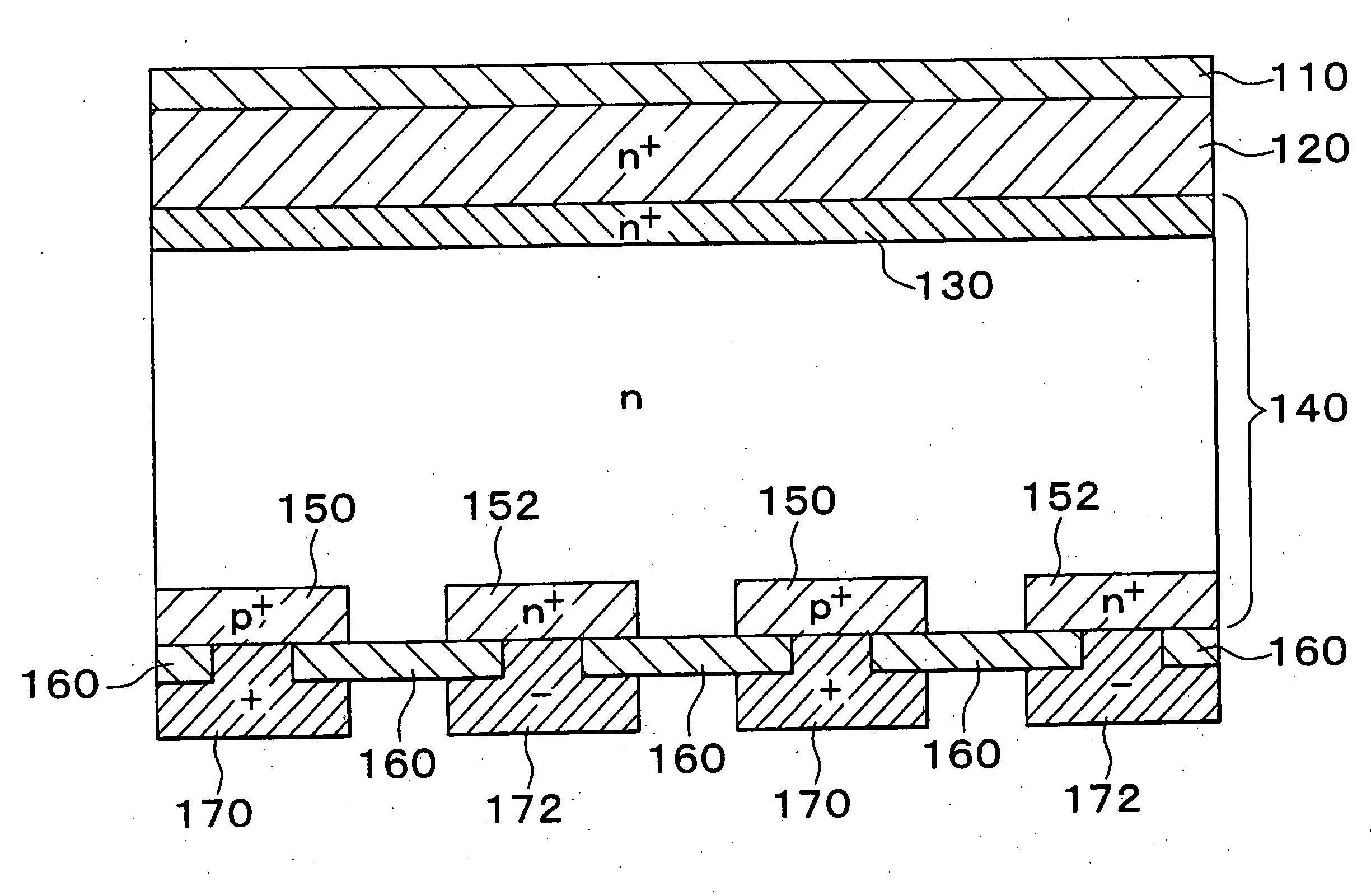
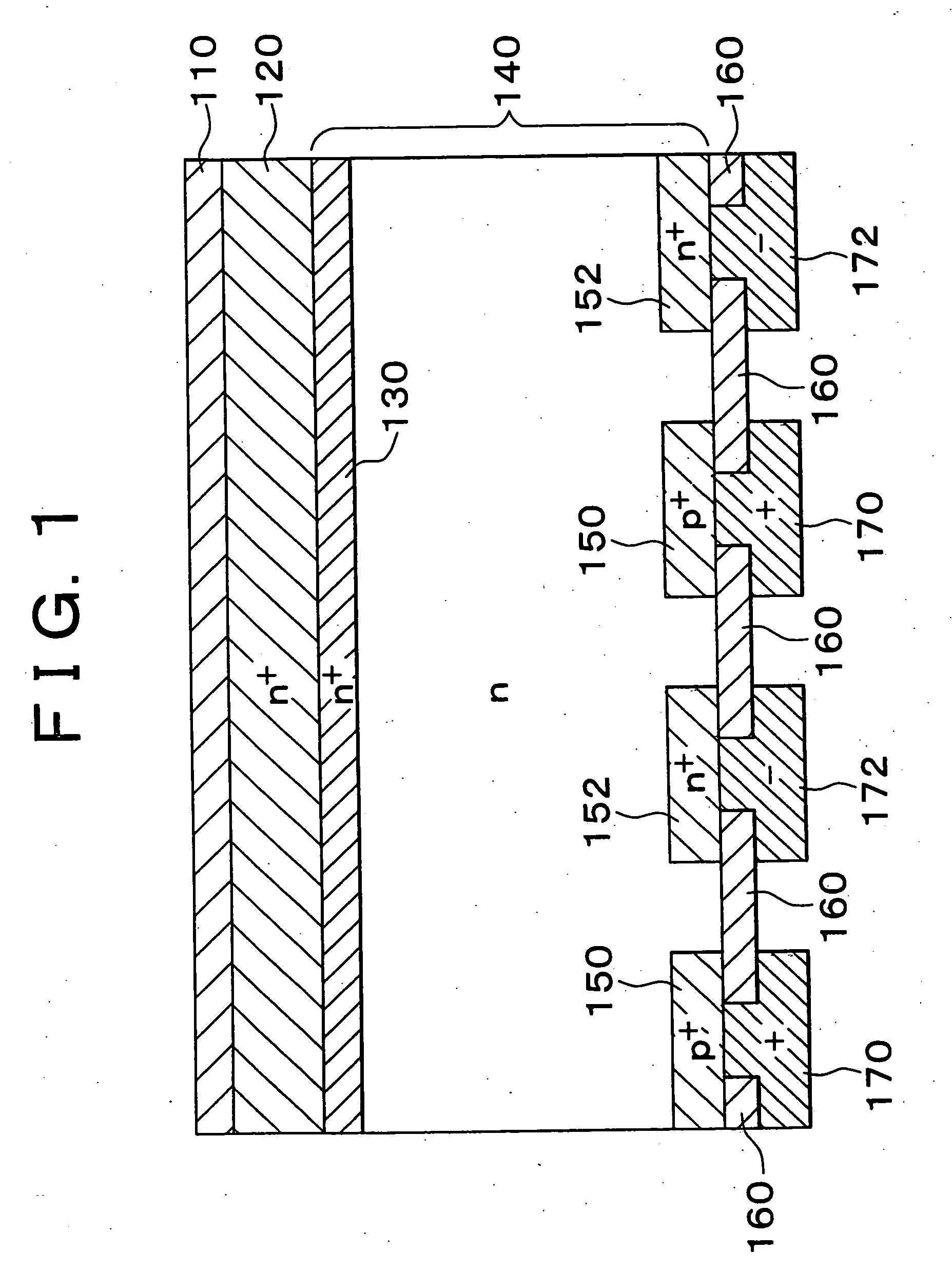
[0034]FIG. 1 is a cross-sectional view of a photoelectric conversion element in accordance with a first embodiment of the invention. First of all, a light-receiving surface side of the basic construction of the photoelectric conversion element shown in FIG. 1 will be described. A reflection-preventing film 110 is a multi-layer optical thin film provided to reduce a light reflection loss. The reflection-preventing film 110 functions as a protective film for protecting a surface of a wide-gap semiconductor thin film 120, which will be described later. The reflection-preventing film 110 reduces the number of defects on an interface between the reflection-preventing film 110 and the semiconductor thin film 120.

[0035] The wide-gap semiconductor thin film 120 is constructed of a semiconductor that is larger in band gap than a semiconductor substrate 140. The wide-gap semiconductor thin film 120 has an element causing a conductivity identical to a conductivity of the semiconductor substra...

second embodiment

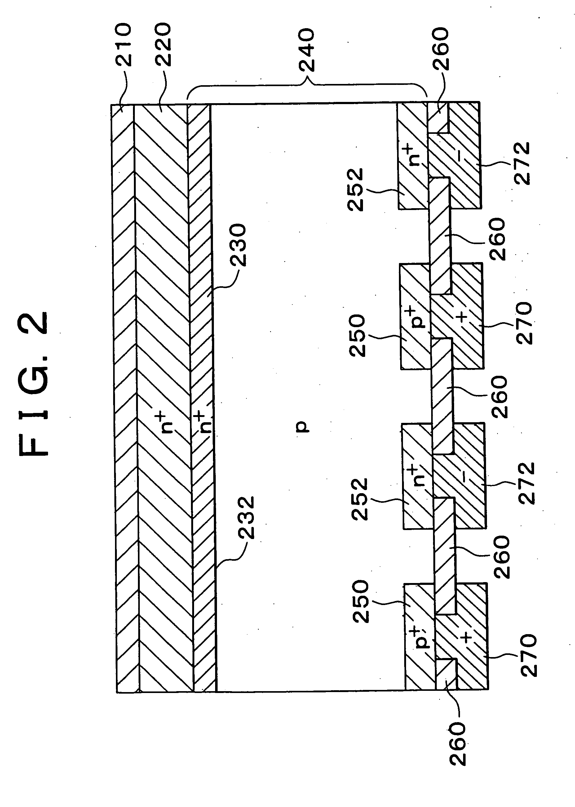
[0050]FIG. 2 is a cross-sectional view of the photoelectric conversion element in accordance with a second embodiment of the invention. First of all, a light-receiving surface side of the basic construction of the photoelectric conversion element shown in FIG. 2 will be described. A reflection-preventing film 210 is substantially the same as the reflection-preventing film 110 of the photoelectric conversion element shown in FIG. 1.

[0051] A wide-gap semiconductor thin film 220 is constructed of a semiconductor that is larger in band gap than a semiconductor substrate 240, and contains an element causing a conductivity that is different from a conductivity of the semiconductor substrate 240.

[0052] In FIG. 2, an upper n30 layer (hereinafter referred to as “a light-receiving surface side n+ layer”) 230 forms a pn junction 232 together with the semiconductor substrate 240, thus controlling a moving direction of carries and reducing a recombination loss on an interface having a large n...

third embodiment

[0067]FIG. 3 is a cross-sectional view of a photoelectric conversion element in accordance with a third embodiment of the invention. First of all, a light-receiving surface side of the basic construction of the photoelectric conversion element shown in FIG. 3 will be described. An insulative thin film 320 is a thin film that allows penetration of 95% or more of light beams having a wavelength of 800 to 2000 nm and that contains an element causing a conductivity identical to a conductivity of a semiconductor substrate 340. The insulative thin film 320 also functions as a reflection-preventing film.

[0068] In FIG. 3, an upper n+ layer (hereinafter referred to as “a light-receiving surface side n+ layer”) 330 controls a moving direction of carriers and reduces a recombination loss on an interface having a large number of defects. The light-receiving surface side n+ layer 330 is formed by the diffusion of an element that is contained in the insulative thin film 320 so as to cause conduc...


PUM


Abstract

In a back-surface electrode type photoelectric conversion element having electrodes and semiconductor layers for collecting carriers disposed only on a back surface side of a semiconductor substrate, a semiconductor thin film that is larger in band gap than the semiconductor substrate and that contains an element causing a conductivity identical to or different from a conductivity of the semiconductor substrate is provided on a light-receiving surface side of the semiconductor substrate, and a diffusion layer is formed on a surface of the semiconductor substrate. Alternatively, 95% or more of light beams having a wavelength of anywhere from 800 nm to 2000 nm are caused to penetrate the light-receiving surface side of the semiconductor substrate, and an insulative thin film containing an element causing a conductivity identical to or different from the conductivity of the semiconductor substrate is provided so as to form a diffusion layer on the surface of the semiconductor substrate through diffusion of the element.

Description

INCORPORATION BY REFERENCE [0001] The disclosure of Japanese Patent Application No. 2001-347808 filed on Nov. 13, 2001, including the specification, drawings, and abstract is incorporated herein by reference in its entirety. BACKGROUND OF THE INVENTION [0002] 1. Field of the Invention [0003] The invention relates to a photoelectric conversion element suited for a thermophotovoltaic power generation device that converts radiant light emitted from a light-emitting body heated by a heat source into electric power by means of a photoelectric conversion element. [0004] 2. Description of the Related Art [0005] As an art for directly obtaining electric energy from fossil fuel or combustible gas, power generation based on thermophotovoltaic energy conversion, namely, thermophotovoltaic power generation (TPV power generation) has been drawing attention. According to the mechanism of TPV power generation, radiant light is generated from a light-emitting body (radiant body or emitter) by apply...

Claims


Application Information

Patent Timeline
Patent Type & Authority Applications(United States)
IPC IPC(8): H01L21/338H01L21/4763H01L21/205H01L27/095H01L29/04H01L31/04H01L31/06H01L31/068H01L31/0725H01L31/074H01L31/0745
CPCH01L31/02167H01L31/0682Y02E10/547H01L31/022441
Inventor NAGASHIMA, TOMONORIOKUMURA, KENICHI
Owner TOYOTA JIDOSHA KK
Learn More