

Photoelectric conversion element and method of manufacturing the same
a technology of photoelectric conversion element and manufacturing method, which is applied in the direction of transistors, solid-state devices, power plants, etc., can solve the problems of unavailing increase light intensity, decrease in light impinging on the photoelectric conversion element, and not quite suited to a photoelectric conversion element, so as to prevent the increase in the number of defects on the surface of the substra
- Summary
- Abstract
- Description
- Claims
- Application Information
AI Technical Summary
Benefits of technology
Problems solved by technology
Method used
Image

Examples
first embodiment
[0034][First Embodiment]
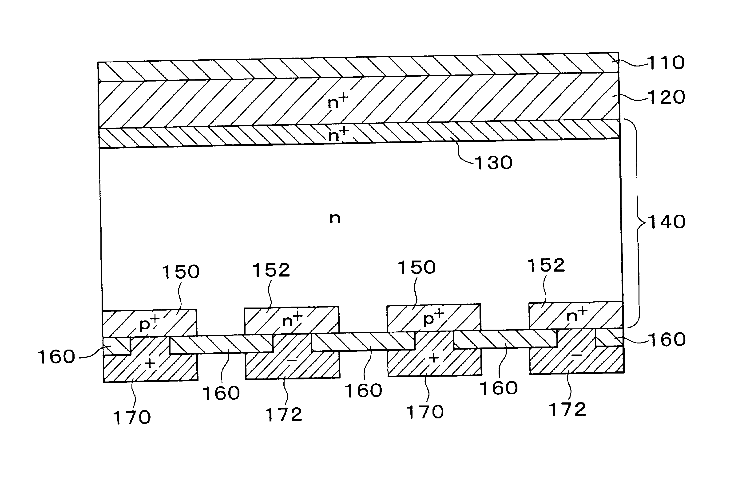
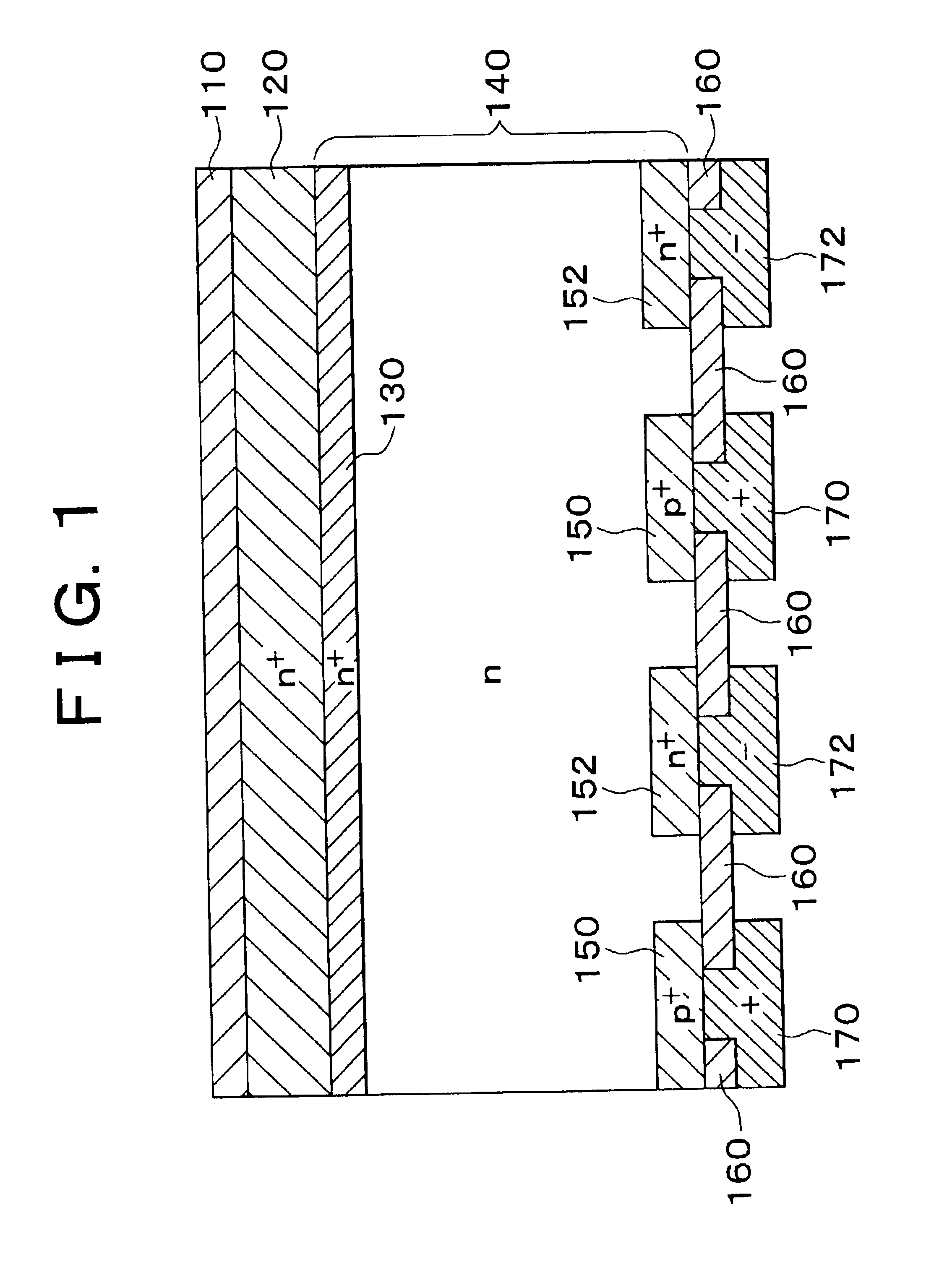
[0035]FIG. 1 is a cross-sectional view of a photoelectric conversion element in accordance with a first embodiment of the invention. First of all, a light-receiving surface side of the basic construction of the photoelectric conversion element shown in FIG. 1 will be described. A reflection-preventing film 110 is a multi-layer optical thin film provided to reduce a light reflection loss. The reflection-preventing film 110 functions as a protective film for protecting a surface of a wide-gap semiconductor thin film 120, which will be described later. The reflection-preventing film 110 reduces the number of defects on an interface between the reflection-preventing film 110 and the semiconductor thin film 120.
[0036]The wide-gap semiconductor thin film 120 is constructed of a semiconductor that is larger in band gap than a semiconductor substrate 140. The wide-gap semiconductor thin film 120 has an element causing a conductivity identical to a conductivity of the...
second embodiment
[0051][Second Embodiment]
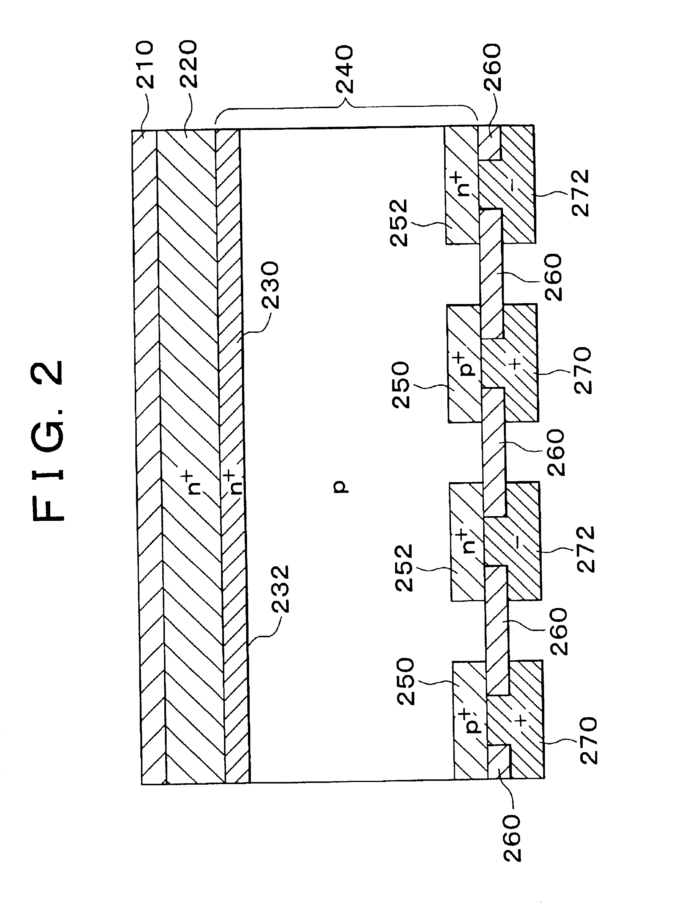
[0052]FIG. 2 is a cross-sectional view of the photoelectric conversion element in accordance with a second embodiment of the invention. First of all, a light-receiving surface side of the basic construction of the photoelectric conversion element shown in FIG. 2 will be described. A reflection-preventing film 210 is substantially the same as the reflection-preventing film 110 of the photoelectric conversion element shown in FIG. 1.
[0053]A wide-gap semiconductor thin film 220 is constructed of a semiconductor that is larger in band gap than a semiconductor substrate 240, and contains an element causing a conductivity that is different from a conductivity of the semiconductor substrate 240.
[0054]In FIG. 2, an upper n+ layer (hereinafter referred to as “a light-receiving surface side n+ layer”) 230 forms a pn junction 232 together with the semiconductor substrate 240, thus controlling a moving direction of carries and reducing a recombination loss on an interfa...
third embodiment
[0069][Third Embodiment]
[0070]FIG. 3 is a cross-sectional view of a photoelectric conversion element in accordance with a third embodiment of the invention. First of all, a light-receiving surface side of the basic construction of the photoelectric conversion element shown in FIG. 3 will be described. An insulative thin film 320 is a thin film that allows penetration of 95% or more of light beams having a wavelength of 800 to 2000 nm and that contains an element causing a conductivity identical to a conductivity of a semiconductor substrate 340. The insulative thin film 320 also functions as a reflection-preventing film.
[0071]In FIG. 3, an upper n+ layer (hereinafter referred to as “a light-receiving surface side n+ layer”) 330 controls a moving direction of carriers and reduces a recombination loss on an interface having a large number of defects. The light-receiving surface side n+ layer 330 is formed by the diffusion of an element that is contained in the insulative thin film 320...
PUM
 Abstract
Description
Claims
Application Information