Magnetic tunnel junction structures and methods of fabrication

a tunnel junction and magnetic tunnel technology, applied in the field of magnetic tunnel junction structures, can solve the problems of undesired variations in magnetic resistance, uneven thickness of layer layers, and poor surface morphology of aluminum oxide layers, etc., to achieve the effect of reducing surface roughness

Inactive Publication Date: 2005-09-22
SAMSUNG ELECTRONICS CO LTD
View PDF50 Cites 40 Cited by
  • Summary
  • Abstract
  • Description
  • Claims
  • Application Information

AI Technical Summary

Benefits of technology

[0011] Exemplary embodiments of the invention provide a method for forming an improved MTJ structure suitable for use in a MRAM device having an improved bottom electrode that provides reduced surface roughness. The improved bottom electrode utilizes a single layer that combines both the seeding layer function and bottom electrode functions of the conventional two-layer structure.

Problems solved by technology

Because the magnetic resistance of an aluminum oxide tunneling layer is exponentially proportional to its thickness, variations in the layer thickness produce even wider and undesired variations in the magnetic resistance.
A bottom electrode 1 formed from a titanium nitride layer as described above tends to exhibit poor surface morphology with a high degree of surface roughness.
When the bottom electrode exhibits a poor surface morphology, the aluminum oxide layer formed above also tends to exhibit a similar poor surface morphology, i.e., a high surface roughness, as a result of the condition of the titanium nitride layer.

Method used


Image

  • Magnetic tunnel junction structures and methods of fabrication
  • Magnetic tunnel junction structures and methods of fabrication
  • Magnetic tunnel junction structures and methods of fabrication

Examples


Embodiment Construction

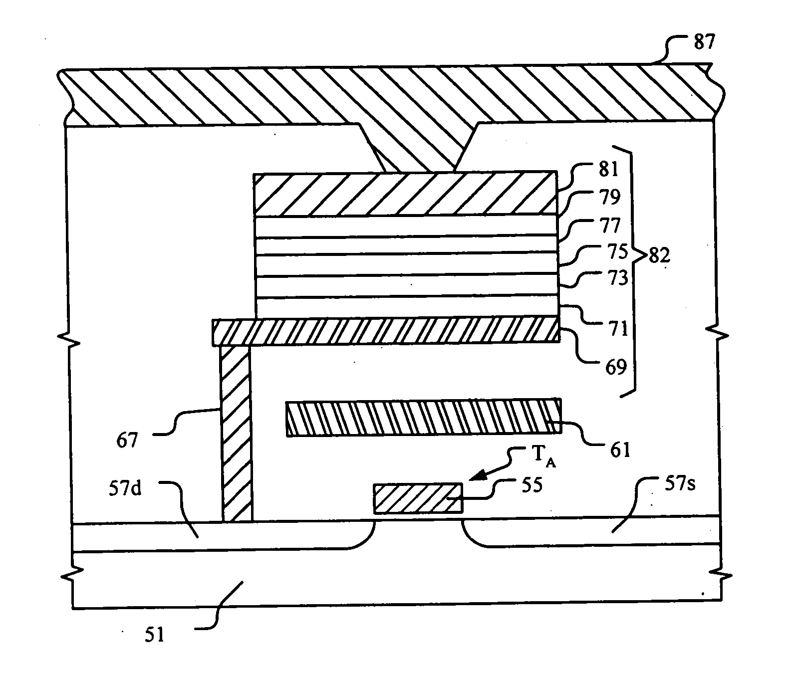
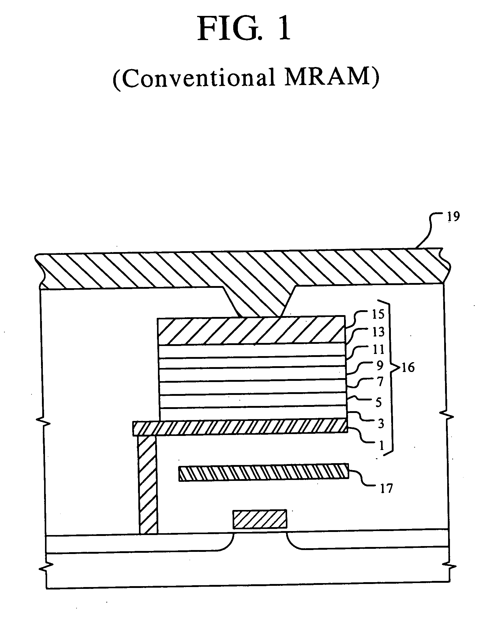
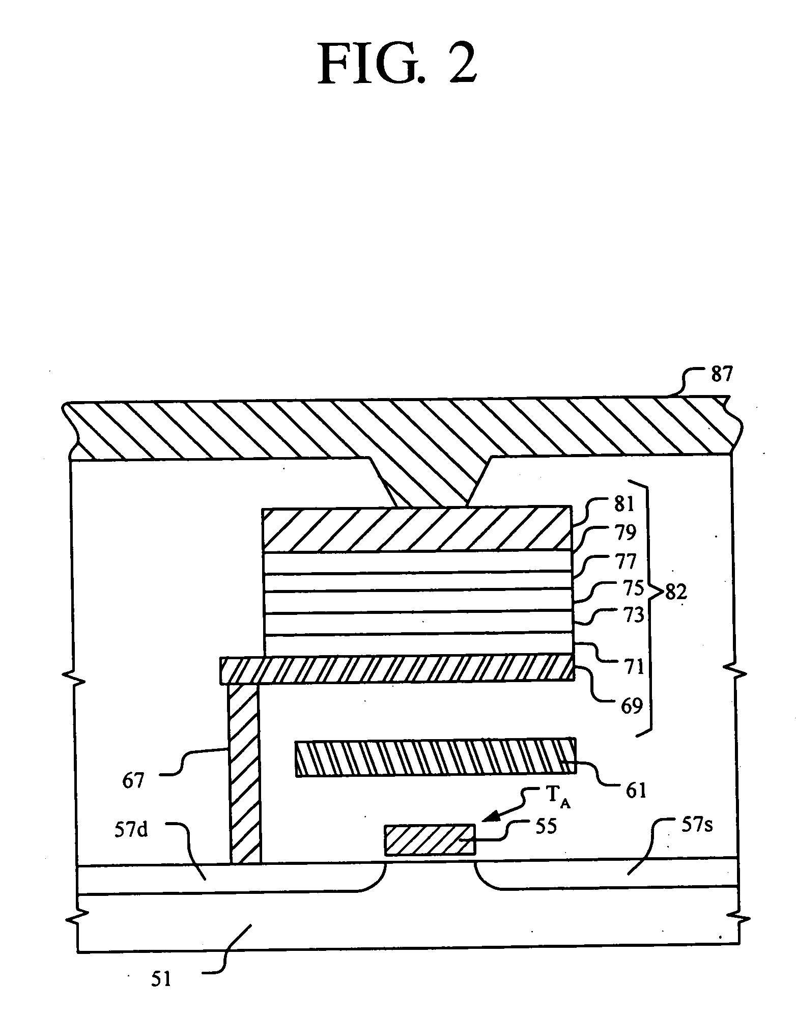
[0017]FIG. 2 is a cross-sectional view illustrating a MRAM cell according to an exemplary embodiment of the invention. As illustrated in FIG. 2, an access transistor TA is formed on a region of a semiconductor substrate 51. The access transistor TA includes a source region 57s and a drain region 57d separated by a channel region with a gate electrode 55 disposed over the channel region and configured to act as a word line. A digit line 61 is located over the access transistor TA and is arranged generally parallel to the word line.

[0018] A magnetic tunnel junction (MTJ) structure 82 is disposed above the digit line 61 and generally opposite the access transistor TA. The MTJ structure 82 is a stacked structure including a bottom electrode 69, a pinning layer pattern 71, a pinned layer pattern 73, a tunneling layer pattern 75, a free layer pattern 77, a capping layer pattern 79 and a top electrode 81. The MTJ structure 82 is insulated from the digit line 61, i.e., an insulating materi...


PUM


Abstract

A method for forming an MTJ structure suitable for use in a MRAM device having a bottom electrode including a layer of platinum, ruthenium, iridium, rhodium, osmium, palladium or their oxides and having reduced surface roughness to improve the hysteresis loop characteristics of the resulting MTJ structure. The bottom electrode layer may also combine the functions of both the seeding layer and bottom electrode of the conventional two-layer structure, thereby simplifying the manufacturing process.

Description

BACKGROUND OF THE INVENTION [0001] 1. Field of the Invention [0002] The present invention relates to magnetic tunnel junction structures suitable for use in magnetic random access memory (MRAM) cells and methods of fabricating such structures, particularly with respect to the bottom electrode of such structures, and is a divisional of application Ser. No. 10 / 376,633, filed Mar. 3, 2003, now allowed, the entire contents of which are incorporated by reference. [0003] 2. Description of the Related Art [0004] Semiconductor memory devices for storing data can generally be categorized as either volatile memory devices or nonvolatile memory devices. Volatile memory devices are those that lose the stored data when their power supplies are interrupted while nonvolatile memory devices are those that retain the stored data even when their power supplies are interrupted. Accordingly, nonvolatile memory devices including flash, static random access memory (SRAM), ferroelectric random access memo...

Claims


Application Information

Patent Timeline
Patent Type & Authority Applications(United States)
IPC IPC(8): G11C11/14H01L27/105G11C11/15H01L21/8234H01L21/8244H01L21/8246H01L27/22H01L43/08H01L43/10H01L43/12
CPCB82Y10/00H01L43/08H01L27/228H10B61/22H10N50/10G11C11/15
Inventor LEE, KYU-MANNKIM, HYUN-JOPARK, JEONG-HEEKIM, TAE-WANSONG, I-HUNCHUNG, SEOK-JAE
Owner SAMSUNG ELECTRONICS CO LTD
Why Eureka
Try Eureka