

Imprint lithography process
- Summary
- Abstract
- Description
- Claims
- Application Information
AI Technical Summary
Benefits of technology
Problems solved by technology
Method used
Image

Examples
Embodiment Construction
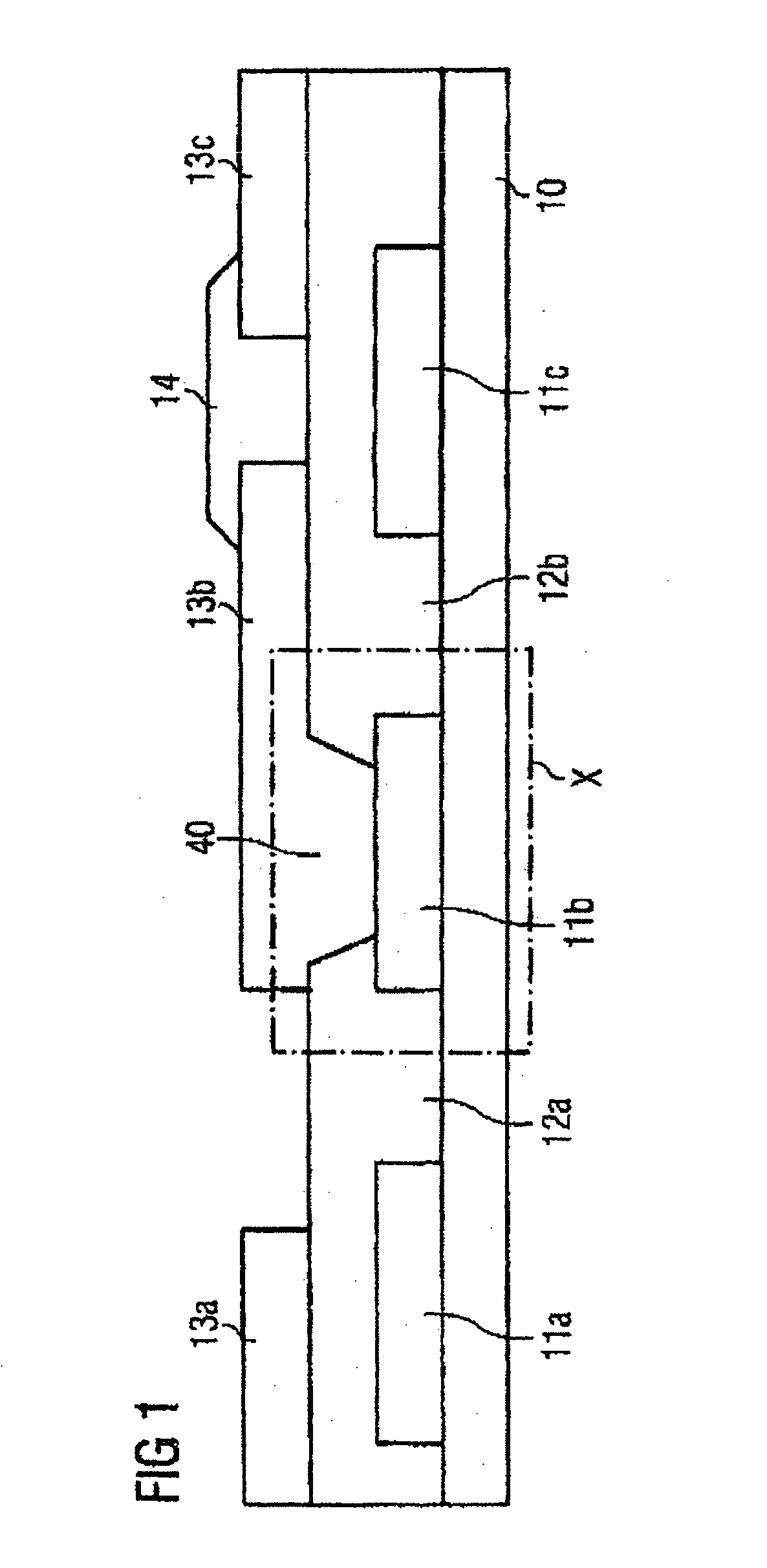
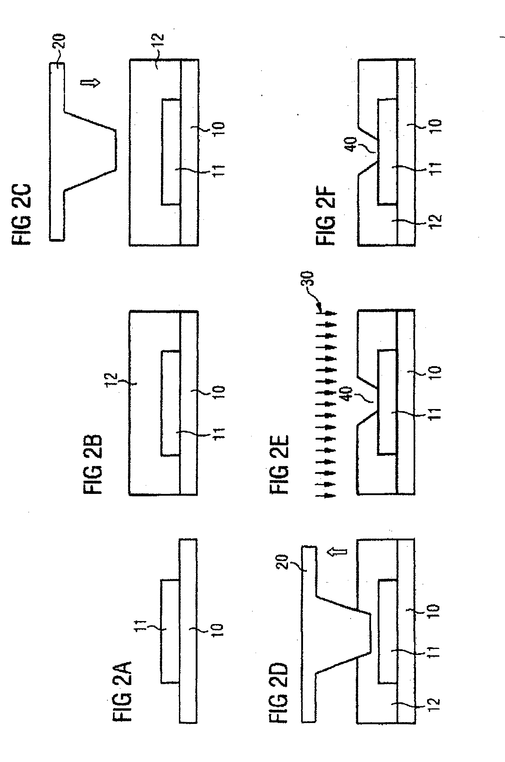
[0090]FIG. 1 shows a schematic cross section through a part of an integrated circuit comprising two conducting layers, namely a first conducting layer 11a, 11b, 11c and a second conducting layer 13a, 13b, 13c present above this. Here, the conducting layers are in the form of metallization planes.
[0091] A gate dielectric layer 12a, 12b and an organic semiconductor layer 14 are arranged above the first conducting layer 11a, 11b, 11c.
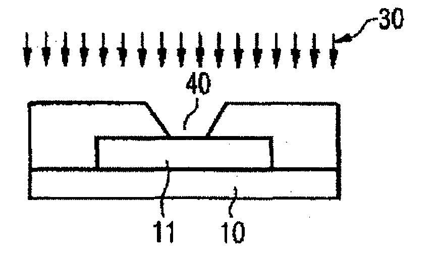
[0092] In order to realize a plated-through hole (“via”), a contact hole 40 must be opened in a targeted manner in the gate dielectric layer 12a, 12b.
[0093] An organic transistor is arranged in the right part of the circuit, consisting of a gate electrode (realized in the first conducting layer 11b, 11c), the gate dielectric 12b, two contacts in the second conducting layer 13b, 13c and the organic semiconductor layer 14.
[0094] A plated-through hole (“via”) is arranged in the middle of the circuit. By opening the contact hole 40, an electrical connectio...
PUM
 Abstract
Description
Claims
Application Information