Solid-state element and solid-state element device

a solid-state element and element technology, applied in the direction of radiation controlled devices, semiconductor devices, electrical apparatus, etc., can solve the problems of electrode layer being separated (peeled) from the semiconductor layer, reducing emission efficiency,

Active Publication Date: 2005-09-29
TOYODA GOSEI CO LTD
View PDF1 Cites 84 Cited by
  • Summary
  • Abstract
  • Description
  • Claims
  • Application Information

AI Technical Summary

Benefits of technology

[0022] It is preferred that the convex portion comprises a h

Problems solved by technology

The Pb free solder has a melting point higher than a Pb containing solder, and therefore a problem is caused that the emission efficiency lowers due to an increase in thermal stress in the flip-chip bonding of LED element.
However, in the above related art 1, there is a problem th

Method used


Image

  • Solid-state element and solid-state element device
  • Solid-state element and solid-state element device
  • Solid-state element and solid-state element device

Examples


first embodiment

(Composition of Light Emitting Device 1)

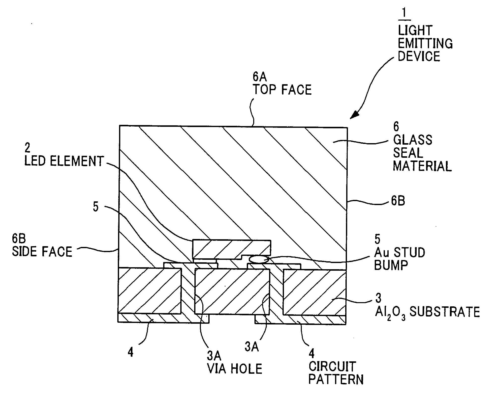
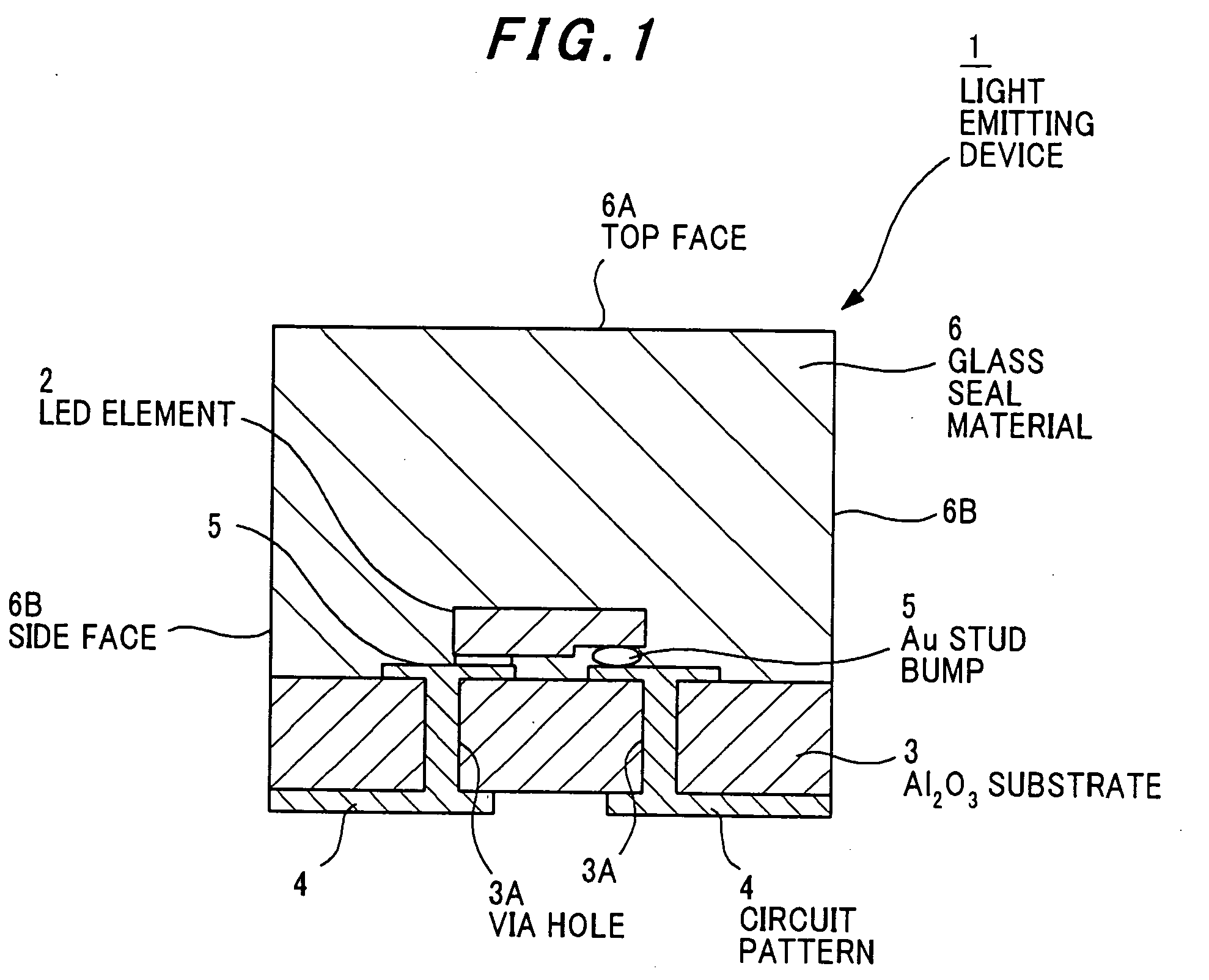
[0076]FIG. 1 is a cross sectional view showing a light emitting device as a solid-state element device in the first preferred embodiment according to the invention.

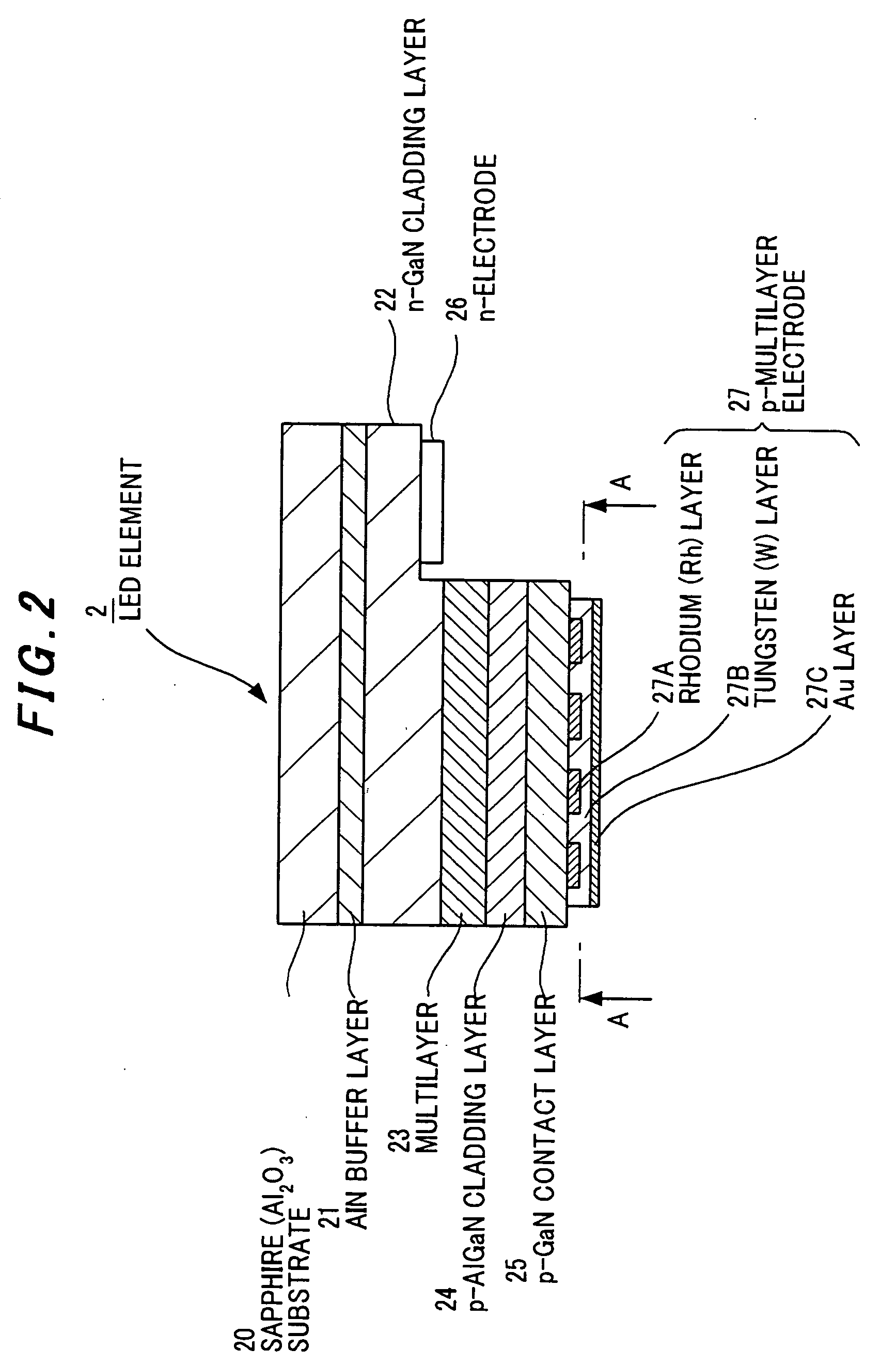
[0077] The light emitting device 1 is composed of: a flip-chip type LED element 2 as a solid-state element that is of GaN based semiconductor; an Al2O3 substrate 3 on which the LED element 2 is mounted; a circuit pattern 4 that is composed of tungsten (W) / nickel (Ni) / gold (Au) and is formed on the Al2O3 substrate 3; an Au stud bump 5 that is formed as a joint portion to connect between the LED element 2 and the circuit pattern 4; and a glass seal material 6 that seals the LED element 2 and is bonded to the Al2O3 substrate 3.

[0078] The Al2O3 substrate 3 is provided with a via hole 3A to electrically connect between the circuit patterns 4 that are of W—Ni and metallized at the front surface and back surface of the substrate 3.

[0079] The glass seal material 6 is of low-melting gla...

second embodiment

(Composition of LED Element 2)

[0096]FIG. 4 is a cross sectional view showing an LED element in the second preferred embodiment according to the invention.

[0097] The LED element 2 of the second embodiment is different from the first embodiment in that a GaN substrate 28 (with a refractive index of n=2.4) is used in place of the sapphire substrate 20 and a Bi based high-refractive index glass with a refractive index of 1.85 is used. The GaN substrate 28 is provided with a slope 28A formed by removing the corner portion by cutting or polishing etc. In this embodiment, like parts are indicated by the same numerals as used in the first embodiment.

(Effects of the Second Embodiment)

[0098] In the second embodiment, adding to the effects of the first embodiment, due to using the GaN substrate 28, the light generated in the multilayer 23 can reach the interface between the GaN substrate 28 and the glass seal material (not shown in FIG. 4) without having an optical loss. Further, since t...

third embodiment

(Composition of LED Element 2)

[0103]FIG. 6A is a cross sectional view showing an LED element in the third preferred embodiment according to the invention. FIG. 6B is a top view showing the LED element in FIG. 6A viewed from a position B in FIG. 6A.

[0104] The LED element 2 is composed of the GaN substrate 28 with the groove 22a formed by cutting on the light discharge surface as explained in FIG. 5A, and the p-multiplayer electrode 27 with the tungsten (W) layer 27B lattice-patterned.

(Effects of the Third Embodiment)

[0105] In the third embodiment, due to the lattice-patterned tungsten (w) layer 27B, the separation of the electrode layer can be prevented. In addition, the p-GaN has a high resistivity, which allows the formation of an emission area according to the pattern of ohmic electrodes, and the uneven surface is formed according to the emission area. Therefore, the light discharge characteristic from the GaN based semiconductor layer can be enhanced.


PUM


Abstract

A solid-state element has: a semiconductor layer formed on a substrate, the semiconductor layer having a first layer that corresponds to an emission area of the solid-state element to and a second layer through which current is supplied to the first layer; a light discharge surface through which light emitted from the first layer is externally discharged, the light discharge surface being located on the side of the substrate; and an electrode having a plurality of regions that are of a conductive material and are in ohmic-contact with the second layer.

Description

[0001] The present application is based on Japanese patent application Nos. 2004-084282, 2004-223600 and 2005-044649, the entire contents of which are incorporated herein by reference. BACKGROUND OF THE INVENTION [0002] 1. Field of the Invention [0003] This invention relates to a solid-state element and a slid-state device and, particularly, to a solid-state element and a slid-state device that prevent the separation of electrode and the reduction of bonding strength cause by a thermal stress so as to discharge efficiently light from inside of the device. [0004] 2. Description of the Related Art [0005] One of conventional solid-state devices is a light emitting device that an LED (light-emitting diode) element as a solid-state element is mounted on a substrate with a lead frame or a wiring pattern. In the light emitting device using the LED element, it is important that light confined inside the LED element is reduced to enhance the external radiation efficiency in order to have a h...

Claims


Application Information

Patent Timeline
IPC IPC(8): H01L27/15H01L29/06H01L29/08H01L29/18H01L29/22H01L29/227H01L29/26H01L31/0256H01L31/12H01L33/06H01L33/32H01L33/38H01L33/40H01L33/62H01L39/22
CPCH01L33/20H01L33/405H01L33/387H01L33/32H01L24/05H01L24/06H01L2224/05568H01L2224/05573H01L2224/05639H01L2224/05644H01L2224/0615H01L2224/14H01L2224/16225H01L2224/17107H01L2924/00014
Inventor SUEHIRO, YOSHINOBUYAMAGUCHI, SEIJI
Owner TOYODA GOSEI CO LTD
Why Eureka
Try Eureka